Introduction
Gold fingers represent a critical feature in printed circuit board design, serving as edge connectors that ensure robust electrical interfaces between PCBs and mating sockets. These gold-plated contacts must withstand repeated insertions and extractions while maintaining low contact resistance and high reliability. In applications ranging from expansion cards to high-speed interfaces, improper gold finger design can lead to intermittent connections, signal integrity issues, or outright failure. Engineers often overlook subtle design rules for gold finger spacing, gold finger length, gold finger alignment, gold finger chamfer, keepout areas for gold fingers, and plated through holes near gold fingers, resulting in manufacturing challenges and field failures. This article explores PCB design rules for gold fingers, highlighting common pitfalls and structured best practices to achieve dependable performance. By adhering to logical engineering principles, designers can optimize these features for long-term reliability.
What Are Gold Fingers and Why Do They Matter
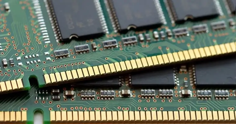
Gold fingers, also known as edge connectors, consist of elongated gold-plated copper traces positioned along the PCB edge to mate with socket contacts. The hard gold plating provides excellent corrosion resistance, low friction, and durability against wear from multiple mating cycles. In electric engineering contexts, they facilitate hot-swappable connections in systems like graphics cards, memory modules, and backplanes, where mechanical stability directly impacts electrical performance. Deviations in PCB design rules for gold fingers can compromise signal integrity, especially in high-frequency applications prone to crosstalk or impedance mismatches. Moreover, gold fingers must align precisely with connector specifications to avoid uneven pressure distribution during insertion. Understanding their role underscores the need for meticulous design to prevent reliability issues in demanding environments.
Key Technical Principles of Gold Finger Design
The engineering foundation of gold fingers lies in their plating process, where electrodeposited hard gold over nickel ensures mechanical robustness and electrical conductivity. Precise gold finger alignment prevents binding or incomplete contact, as misalignment shifts contact forces unevenly across the interface. Gold finger length must extend sufficiently into the socket for stable overlap, balancing mechanical retention with avoidance of excessive protrusion that could cause bending. Spacing between individual fingers controls crosstalk and allows for uniform plating coverage during manufacturing. Chamfering the PCB edge adjacent to gold fingers reduces insertion force and minimizes damage to plating or substrate. Keepout areas for gold fingers define zones free of other features to safeguard plating integrity and routing flexibility.
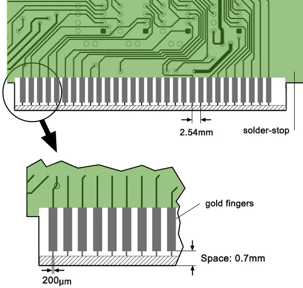
Gold finger spacing requires careful consideration to match the pitch of the target connector while providing clearance for plating processes. Inadequate spacing risks bridging during electroplating or solder mask application, leading to shorts. Conversely, excessive spacing may necessitate wider boards, impacting system density. Engineers should verify spacing tolerances against connector datasheets early in the design phase. Proper implementation ensures consistent electrical performance across production lots.
Gold Finger Length and Alignment Considerations
Gold finger length determines the contact area's effectiveness, requiring enough extension to engage fully with socket beams without overhanging. Short lengths result in partial contact and higher resistance, while overly long fingers invite mechanical stress during mating. Alignment demands parallelism across all fingers, as even minor angular deviations amplify at the edge, causing localized wear. Fabrication tolerances for etching and plating influence alignment precision, necessitating design margins. Electrical testing post-assembly reveals alignment flaws through contact resistance measurements. Structured design reviews incorporating simulation tools help predict and mitigate these issues.
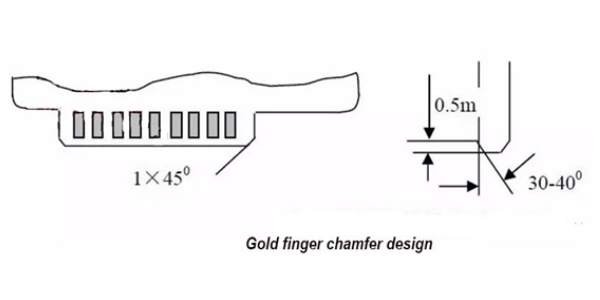
Importance of Gold Finger Chamfer and Edge Beveling
The gold finger chamfer, typically implemented as a beveled edge on the PCB, facilitates smooth insertion by guiding the board into the socket. Without proper chamfering, sharp edges scrape against socket contacts, damaging gold plating or dislodging debris into the interface. Bevel angles must suit the board thickness and connector geometry to distribute insertion forces evenly. Inadequate chamfer depth exposes unprotected substrate, accelerating wear over cycles. Manufacturing processes like routing or milling achieve the bevel post-plating to preserve surface finish. Logical selection of chamfer parameters enhances mating reliability in high-cycle applications.
Defining Keepout Areas for Gold Fingers
Keepout areas for gold fingers establish exclusion zones around the contacts to prevent interference from vias, traces, or components. These regions accommodate beveling tools and plating racks, avoiding contamination or mechanical damage. Neglecting keepouts leads to exposed copper or solder mask encroachment, compromising plating uniformity. Designers define keepouts extending from the finger base inward, coordinating with layer stackup to remove inner-layer copper beneath. This practice aligns with PCB design rules for gold fingers by isolating the edge region. Verification through design rule checks ensures compliance throughout layout iterations.
Risks of Plated Through Holes Near Gold Fingers
Plated through holes near gold fingers pose significant risks due to plating chemistry migration during electroplating. Proximity allows gold or nickel to deposit into via barrels, causing shorts or reliability degradation under thermal stress. Mechanical beveling may also nick nearby PTH barrels, exposing barrel plating to corrosion. Industry guidance recommends sufficient separation to isolate processes, with keepouts encompassing PTH exclusion. Routing adjustments or blind vias serve as alternatives in dense designs. Adhering to these PCB design rules for gold fingers prevents field failures linked to interconnection defects.
Common Pitfalls in Gold Finger Implementation
Misaligned gold fingers often stem from panelization errors or routing inaccuracies, manifesting as high contact resistance or intermittent connectivity. Insufficient gold finger length fails to provide redundant contact points, exacerbating wear in vibration-prone environments. Poor gold finger spacing invites plating defects like bridging or porosity, detectable via visual inspection per IPC-A-600 criteria. Inadequate chamfering results in insertion damage, with beveled edges chipping solder mask or plating layers. Overlooking keepout areas for gold fingers permits PTH encroachment, leading to electrochemical issues. Plated through holes near gold fingers frequently cause yield losses during beveling or final assembly.
Engineers encounter warpage-related pitfalls where board flexure misaligns fingers during mating. Thermal expansion mismatches between plating and substrate induce cracking over time. Fabrication tolerances amplify small design errors, such as non-parallel fingers. Troubleshooting involves cross-section analysis to inspect plating adhesion and thickness uniformity. Proactive design simulations model insertion dynamics and stress distribution. Correcting these pitfalls requires iterative verification against IPC-6012 performance specifications.
Best Practices for Reliable Gold Finger Design
Establish precise gold finger spacing matching the connector pitch, incorporating margins for fabrication tolerances. Optimize gold finger length for full socket engagement, typically extending beyond the contact beam centerline. Ensure gold finger alignment through symmetric routing and fiducial marks for panel registration. Implement gold finger chamfer with consistent beveling across the edge, coordinating with board thickness. Define comprehensive keepout areas for gold fingers, prohibiting PTHs, traces, and mask within specified zones. Avoid plated through holes near gold fingers by relocating or using blind/buried vias.
Layer stackup management removes copper under gold fingers to prevent telegraphing during plating. Solder mask openings extend to the board edge, avoiding coverage on contact surfaces. Post-plating beveling preserves plating integrity, with edge plating controlled for uniformity. Design for testability includes probe-safe areas away from fingers. Compliance with IPC-2221 design guidelines structures these practices logically. Final DFM reviews confirm adherence to PCB design rules for gold fingers.
Troubleshooting Gold Finger Issues
When gold finger alignment fails, inspect panel fiducials and routing paths for offsets. Measure contact resistance across cycles to quantify performance degradation from spacing errors. Visual anomalies like pitting signal plating issues tied to keepout violations. Simulate insertion forces to diagnose chamfer inadequacies. Cross-sections reveal PTH proximity effects on barrel plating. Systematic root cause analysis restores reliability.
Conclusion
Mastering PCB design rules for gold fingers demands attention to spacing, length, alignment, chamfer, keepouts, and PTH placement for uncompromised connections. Avoiding pitfalls through structured engineering practices ensures durability in high-reliability applications. Logical integration of these elements aligns with industry standards, minimizing risks from manufacturing to field use. Designers benefit from early verification and DFM collaboration. Reliable gold fingers enhance overall system performance, supporting electric engineers in demanding designs.
FAQs
Q1: What is the importance of gold finger spacing in PCB design?
A1: Proper gold finger spacing prevents electrical crosstalk and ensures uniform plating during manufacturing. Inadequate spacing risks shorts or uneven contact pressure in sockets. Engineers match spacing to connector pitch while allowing process margins. This PCB design rule for gold fingers upholds signal integrity in high-density interfaces. Adherence reduces rework and enhances yield.
Q2: How does gold finger chamfer affect insertion reliability?
A2: Gold finger chamfer bevels the PCB edge to guide smooth mating, reducing friction and plating wear. Common angles facilitate even force distribution across contacts. Without chamfer, sharp edges damage sockets or fingers over cycles. This feature integrates with keepout areas for gold fingers to protect adjacent features. Optimal chamfer design prolongs connector lifespan.
Q3: Why avoid plated through holes near gold fingers?
A3: Plated through holes near gold fingers risk plating contamination and mechanical damage during beveling. Migration of gold into vias causes shorts or reliability failures. Keepout areas for gold fingers enforce separation for process isolation. Relocating PTHs or using advanced vias maintains integrity. This rule is essential for PCB design rules for gold fingers in multilayer boards.
Q4: What role does gold finger alignment play in performance?
A4: Gold finger alignment ensures even contact across all traces, preventing localized high resistance or wear. Misalignment from routing errors amplifies during insertion. Fiducials and symmetric layouts aid precision. Verification confirms compliance with connector specs. Strong alignment supports repeated cycles without degradation.
References
IPC-6012E — Qualification and Performance Specification for Rigid Printed Boards. IPC, 2017
IPC-A-600K — Acceptability of Printed Boards. IPC, 2020
IPC-2221F — Generic Standard on Printed Board Design. IPC, 2012
IPC-4556 — Specification for Electrodeposited Au over Ni/NiPd for Printed Circuit Boards. IPC, 2015


