Introduction
In the evolving landscape of printed circuit board (PCB) manufacturing, laser drilling has become indispensable for producing high-density interconnects (HDI) PCBs. This technique enables the creation of microvias and precise vias that support the miniaturization demands of modern electronics. Electric engineers designing compact devices such as smartphones, wearables, and automotive modules increasingly rely on laser-drilled features to achieve superior routing density and signal integrity. Unlike traditional mechanical drilling, laser drilling offers non-contact precision that minimizes material stress and enables aspect ratios suitable for blind and buried vias. As PCB complexity grows, understanding the PCB laser drilling process becomes essential for optimizing designs and ensuring manufacturability. This article explores how laser drilling works, its benefits, and key PCB applications, providing factory-driven insights aligned with industry practices.
What Is PCB Laser Drilling and Why It Matters
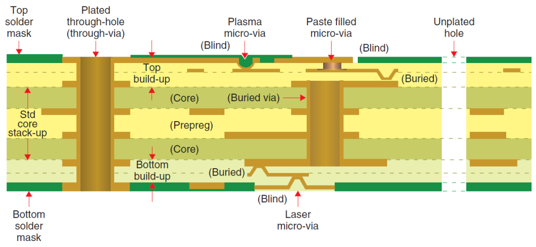
PCB laser drilling involves using a focused laser beam to ablate material and form vias or holes in the board substrate. It primarily targets dielectric layers and copper pads to create microvias, defined as blind vias with a maximum aspect ratio of 1:1 according to IPC-T-50. This process matters because mechanical drilling struggles with holes smaller than 100 microns, limiting density in HDI PCBs where microvias connect adjacent layers efficiently. In high-performance applications, laser drilling reduces via stubs, improving signal speed and electromagnetic compatibility. Factory production lines integrate laser drilling to meet the demands of fine-pitch components like BGAs, enabling shorter interconnect paths. Ultimately, it drives the transition from standard multilayer boards to advanced HDI structures essential for next-generation electronics.
Laser drilling's relevance extends to quality control in manufacturing, where it supports compliance with specifications for via reliability under thermal stress. Engineers must consider it early in design to avoid rework, as microvia placement directly impacts layer count and board size. Without laser capabilities, achieving high I/O density becomes impractical, underscoring its role in sustaining Moore's Law in PCB form.
The PCB Laser Drilling Process Explained
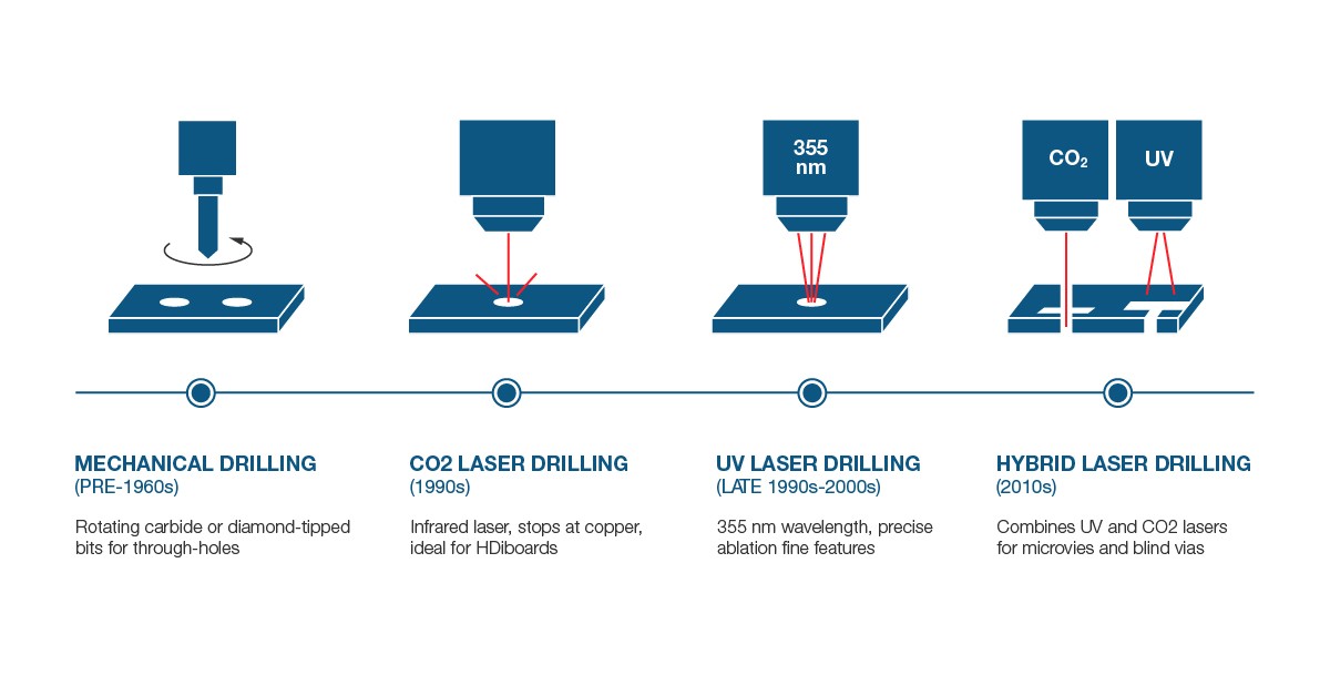
The PCB laser drilling process begins with aligning the board under a stationary laser system programmed for specific hole locations from Gerber data. A high-energy beam, typically from CO2 or UV lasers, focuses on the target area to vaporize dielectric material through ablation. CO2 lasers, operating at 9-10 micron wavelengths, excel at removing organics like epoxy resins in FR-4 substrates by heating and gasifying the material rapidly. Pulses are delivered in bursts, with each removing a thin layer until the desired depth is reached, often stopping at a copper landing pad. UV lasers, with shorter wavelengths around 355 nm, are preferred for copper drilling due to their ability to photoablate metals without excessive heat-affected zones.
Following ablation, desmear processes clean residues using plasma or chemical treatments to ensure plating adhesion. The system controls parameters like fluence (energy per area), pulse duration, and repetition rate to achieve tapered or straight barrel profiles. Quality verification occurs via automated optical inspection (AOI) for hole diameter, taper angle, and cleanliness. This digital control allows batch processing of thousands of vias per panel with sub-micron repeatability. In HDI builds, sequential lamination integrates laser drilling between build-up layers, forming stacked or staggered microvias.
Key Laser Drilling Benefits for PCB Manufacturing
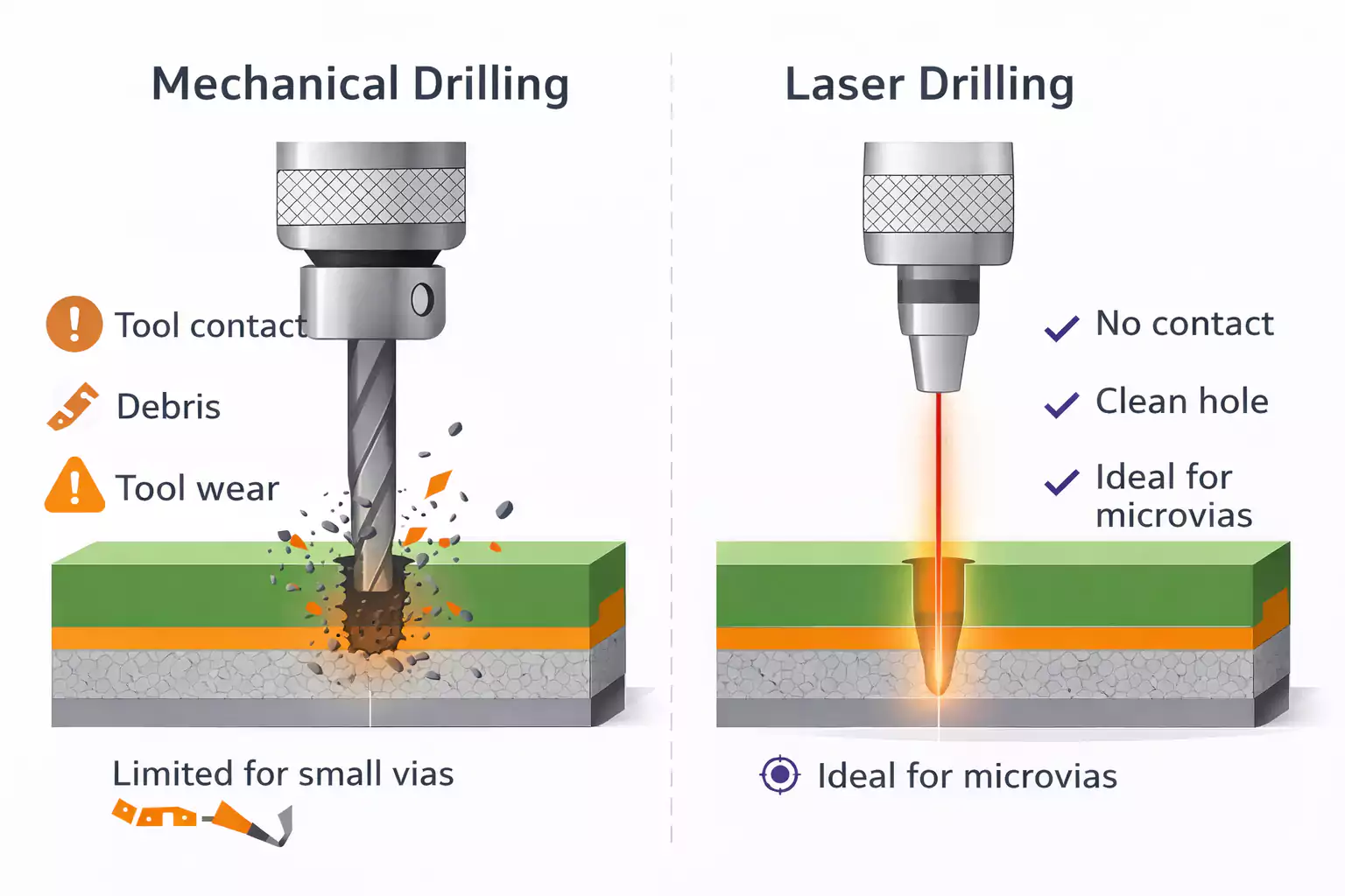
One primary laser drilling benefit is unparalleled precision, enabling microvias as small as 40-50 microns in diameter, far beyond mechanical limits. This supports HDI PCBs with via-in-pad configurations, maximizing routable area under dense BGA footprints. Non-contact processing eliminates drill bit wear, burrs, and mechanical stress that can cause microcracks in thin cores. Factories report consistent hole quality across panels, reducing scrap rates compared to high-speed mechanical drills prone to wander in small diameters.
Laser drilling also enhances thermal management by producing cleaner hole walls for better plating uniformity, crucial for current carrying capacity. It facilitates blind and buried vias, shortening signal paths and minimizing inductance for high-frequency designs up to GHz ranges. Reduced layer counts in HDI stacks lower material costs and weight, benefiting portable devices. Environmentally, it generates less waste than mechanical methods due to no consumable bits.
Another advantage lies in material versatility; lasers handle high-Tg resins, polyimides, and buildup films without delamination risks. Overall, these laser drilling benefits translate to higher yields and faster time-to-market in production.
Applications of Laser Drilling in Modern PCBs
In HDI PCBs, laser drilling forms the backbone for microvias in consumer electronics like smartphones and smartwatches, where space constraints demand stacked via architectures. These microvias enable fanout from 0.3 mm pitch BGAs, connecting surface pads directly to inner layers per IPC-2226 guidelines for high-density designs. Automotive ECUs and ADAS modules leverage laser-drilled blind vias for reliable power distribution amid vibration and thermal cycling.
Medical devices, such as implantable pacemakers, utilize laser precision for hermetic seals and minimal size. Aerospace applications employ it for lightweight, high-reliability boards with buried vias reducing EMI. Telecommunications routers benefit from staggered microvias, supporting 5G signal integrity with low loss.
Laser drilling extends to flexible and rigid-flex PCBs, drilling vias in polyimide dielectrics for wearables. In servers and data centers, it densifies backplanes for AI accelerators. Across these PCB applications, microvias stack to six or more layers, enabling complexity classes 4-6 in HDI per industry classifications.
Best Practices and Quality Control in PCB Laser Drilling
To optimize the PCB laser drilling process, engineers should specify via sizes and locations adhering to IPC-6016 qualification standards for HDI boards. Select laser type based on stackup: CO2 for bulk dielectric removal, UV for copper direct drilling to avoid residue. Program overlap factors to control taper, typically 10-15 degrees for plating ease, and maintain fluence below material damage thresholds.
Post-drill desmear is critical; plasma etching removes smear without enlarging holes, followed by permanganate if needed. Implement in-line metrology like laser triangulation for depth measurement and SEM cross-sections for reliability validation. Control environmentals—temperature and humidity—to prevent condensation on panels.
Quality control routines include electrical testing of plated vias and thermal shock per J-STD-020 for moisture sensitivity. Monitor via covariance; aim for under 5% variation in diameter. Factory protocols often incorporate statistical process control (SPC) charting pulse counts versus hole metrics. These practices ensure microvia reliability exceeding 1 million cycles.
Conclusion
PCB laser drilling revolutionizes manufacturing by enabling microvias essential for HDI PCBs and compact designs. Its precise, non-contact ablation delivers cleaner holes, higher density, and better performance than mechanical alternatives. Electric engineers benefit from shorter paths, reduced layers, and versatile applications across industries. Adhering to best practices and standards like IPC-2226 ensures robust production outcomes. As electronics miniaturize further, laser drilling will remain central to advancing PCB capabilities.
FAQs
Q1: What is the PCB laser drilling process for creating microvias?
A1: The process uses focused CO2 or UV laser pulses to ablate dielectric and copper, forming blind vias between layers. Parameters like energy density and pulse repetition control depth and shape. Desmear follows to prepare for plating, ensuring HDI PCB reliability. This enables diameters under 75 microns with 1:1 aspect ratios.
Q2: What are the main laser drilling benefits for HDI PCBs?
A2: Key benefits include precision for tiny microvias, no mechanical damage, and increased routing density. It supports stacked vias, reduces signal loss, and handles diverse materials. Factories achieve higher yields with consistent plating quality, vital for high-frequency PCB applications.
Q3: In which PCB applications is laser drilling most common?
A3: Laser drilling shines in HDI PCBs for smartphones, automotive electronics, and medical implants needing microvias. It facilitates fine-pitch BGA fanout and multilayer stacking. Aerospace and telecom also rely on it for EMI control and compactness.
Q4: How does quality control ensure reliable laser-drilled microvias?
A4: Control involves AOI for dimensions, cross-section analysis for walls, and electrical tests post-plating. Standards like IPC-6016 guide acceptance criteria for taper and cleanliness. SPC monitors process stability, minimizing defects in production.
References
IPC-2226A — Sectional Design Standard for High Density Interconnects. IPC.
IPC-6016E — Qualification and Performance Specification for High Density Interconnect (HDI) Printed Boards. IPC.
IPC-T-50P — Terms and Definitions for Interconnecting and Packaging Electronic Circuits. IPC.


