Introduction
PCB laser drilling has become essential in modern electronics manufacturing, particularly for producing high-density interconnect (HDI) boards. This process enables the creation of precise microvias that support denser routing and smaller form factors. Electric engineers rely on laser drilling to meet the demands of compact devices like smartphones, wearables, and automotive electronics. By using focused laser beams, manufacturers achieve hole sizes and tolerances unattainable with mechanical methods. This article explores PCB laser drilling materials, laser drilling techniques, and PCB equipment, providing factory-driven insights aligned with industry standards.
What Is PCB Laser Drilling and Why It Matters
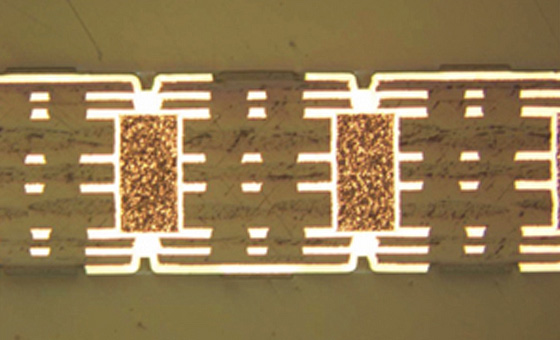
PCB laser drilling involves directing a high-energy laser beam to ablate material and form vias or holes in printed circuit boards. Unlike mechanical drilling, which uses rotating bits prone to wear and breakage at small diameters, laser drilling offers non-contact precision. This method excels in creating blind, buried, and through-hole vias with diameters as small as those required for HDI boards. Its importance stems from the need for higher interconnect density in advanced PCBs, where traditional drilling limits miniaturization.
In HDI fabrication, laser drilling supports sequential build-up processes, allowing multiple layers of microvias. Compliance with standards like IPC-2226 ensures design feasibility and manufacturability. Factory experience shows that laser-drilled vias reduce signal path lengths, improving electrical performance and thermal management. For electric engineers, understanding this process optimizes designs for reliable production yields.
PCB Laser Drilling Materials
Selecting appropriate PCB laser drilling materials is critical for achieving clean ablation and via quality. Standard epoxy-based laminates like FR-4 are widely used due to their compatibility with laser energy absorption. These materials consist of woven glass cloth impregnated with resin, which vaporizes predictably under laser exposure. However, glass fibers can cause inconsistencies if not properly matched to the laser wavelength.
Advanced materials such as polyimide offer superior thermal stability for high-reliability applications. PTFE-based laminates suit high-frequency designs, though they require careful parameter tuning to avoid charring. Resin-coated copper (RCC) and photoimageable dielectrics provide smooth surfaces for direct laser drilling without pre-etching. Factory insights emphasize using laser-drillable prepregs to minimize taper and residue, ensuring plating adhesion post-drilling.
Certain composites with ceramic fillers demand higher energy densities, but they expand HDI capabilities in harsh environments. Engineers must verify material datasheets for laser absorptivity at specific wavelengths. Poor compatibility leads to heat-affected zones, compromising IPC performance criteria.
Laser Drilling Techniques
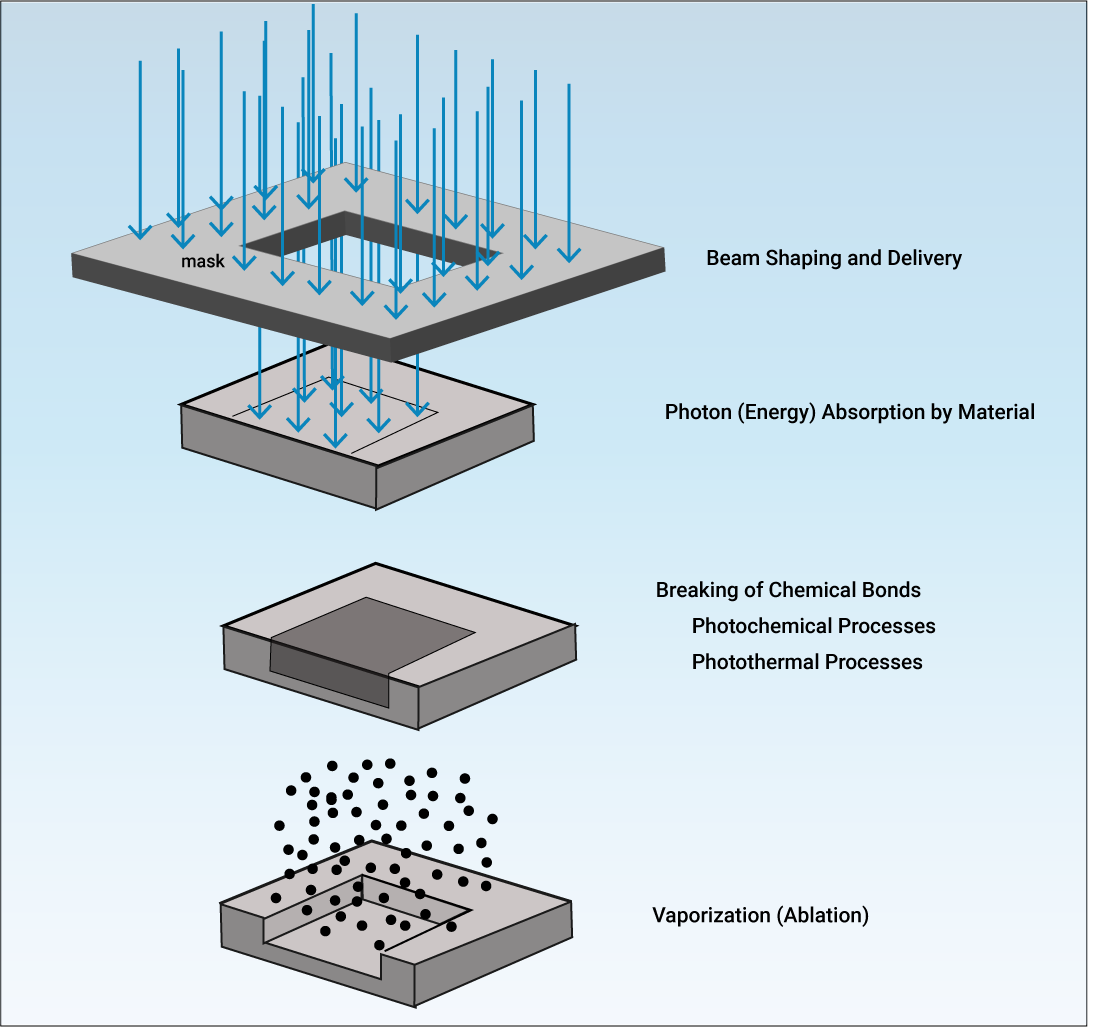
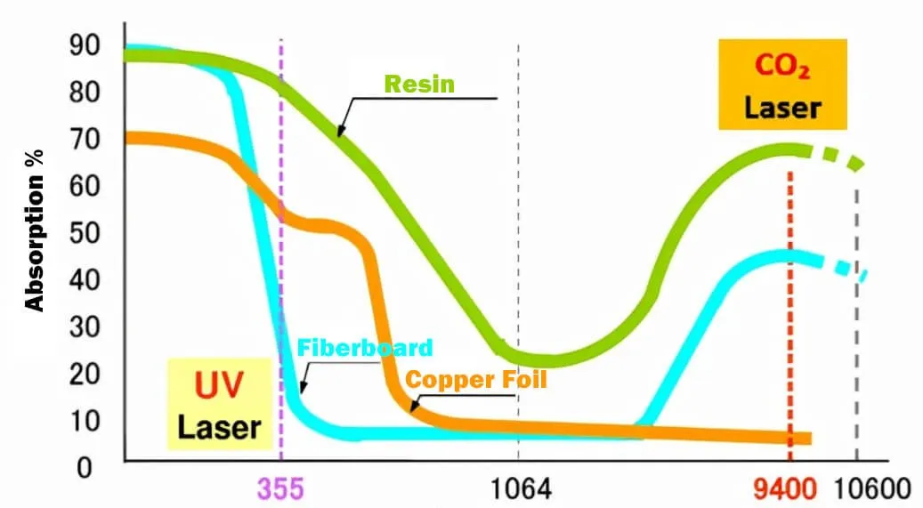
Laser drilling techniques primarily revolve around ablation, where photons break molecular bonds to remove material vapor. CO2 lasers, operating at around 10.6 micrometers wavelength, excel in dielectric drilling due to strong organic absorption. The beam thermally vaporizes resin, stopping at copper layers because of the metal's reflectivity. This makes CO2 ideal for through-hole and larger blind vias in multilayer boards.
UV lasers, typically at 355 nanometers, enable cold ablation with minimal thermal damage. Their high photon energy cleanly removes thin copper foil first, followed by dielectric. This precision suits stacked microvias in HDI boards, achieving aspect ratios near 1:1 as per IPC-2226 guidelines. Pulsed operation controls depth, preventing over-drilling.
Hybrid approaches combine both lasers in sequence for complex stackups. Laser ablation parameters like pulse duration, repetition rate, and fluence determine hole geometry. Factory processes include fiducial alignment for accuracy and gas assist to clear debris.
PCB Equipment for Laser Drilling
PCB equipment for laser drilling features robust systems with galvo scanners for rapid beam positioning. The core is the laser source, either CO2 tube or UV solid-state, integrated with optics for beam shaping. Motion stages handle panel fixturing, often in vacuum or cleanroom environments to control particulates.
Advanced setups include vision systems for auto-registration and process monitoring via inline metrology. Power supplies and chillers maintain stability during high-volume production. Software programs drill patterns, optimizing hit counts per via for uniform taper.
Equipment calibration ensures repeatability, aligning with IPC-TM-650 test methods for via geometry. Electric engineers appreciate modular designs allowing wavelength swaps for material versatility. Throughput reaches thousands of vias per panel, supporting HDI economies of scale.
Best Practices for PCB Laser Drilling
Implement design rules from IPC-2226 to maximize yields, such as limiting microvia aspect ratios and staggering vias across layers. Specify laser-drillable materials early to avoid rework. Optimize drill parameters through test coupons, adjusting energy for entry-exit cleanliness.
Post-drill desmear removes residue using plasma or permanganate, preparing for plating. Inspect vias with cross-sectioning or electrical testing per IPC standards. Factory best practices include multi-hit strategies for deeper vias and coolant use to dissipate heat.
Monitor equipment with preventive maintenance to prevent pulse degradation. Collaborate with fabricators on panel size and stackup feasibility. These steps ensure robust HDI boards with reliable laser-drilled features.
Troubleshooting Common Issues in Laser Drilling
Residue buildup often traces to incompatible materials or insufficient desmear. Increase pulse energy or add plasma cleaning cycles. Tapered vias result from defocusing; recalibrate galvo optics.
Copper smear on dielectric indicates UV underpower; boost fluence for clean breakthrough. Heat-affected zones in sensitive laminates call for shorter pulses. Cross-reference issues against IPC-TM-650 methods for root cause analysis.
Panel warpage post-drilling requires symmetric via placement and build-up sequencing. Electric engineers can mitigate by simulating thermal stresses in design phase.
Conclusion
PCB laser drilling revolutionizes HDI board production through precise materials handling, advanced techniques like UV and CO2 ablation, and specialized equipment. Electric engineers benefit from its enablement of denser, higher-performance designs. Adhering to standards ensures quality and reliability. As demands for miniaturization grow, mastering these elements drives manufacturing success.
FAQs
Q1: What materials are best for PCB laser drilling materials in HDI applications?
A1: FR-4 epoxy laminates, polyimide, and RCC provide excellent compatibility due to their ablation properties. PTFE suits high-frequency needs but requires tuned parameters. Always select laser-drillable prepregs to ensure clean vias and plating adhesion, aligning with factory processes for HDI boards.
Q2: How do laser drilling techniques differ for CO2 and UV lasers?
A2: CO2 lasers use thermal ablation for dielectrics, stopping at copper reflectivity, ideal for larger vias. UV lasers perform cold ablation, cleanly penetrating thin copper and dielectric for microvias. Choose based on stackup; hybrids optimize complex HDI laser drilling techniques.
Q3: What PCB equipment features enhance laser drilling precision?
A3: Galvo scanners, vision alignment, and pulsed sources deliver sub-micron accuracy. Inline metrology monitors via quality. Cleanroom integration controls debris, supporting high-volume HDI production with reliable PCB equipment.
Q4: Why is laser ablation critical for HDI boards?
A4: Laser ablation creates microvias under 150 micrometers, enabling dense interconnects unattainable mechanically. It supports blind and stacked vias in sequential build-ups, improving signal integrity per IPC guidelines.
References
IPC-2226 — Sectional Design Standard for HDI Printed Boards. IPC.
IPC-6012E — Qualification and Performance Specification for Rigid Printed Boards. IPC, 2017.
IPC-TM-650 — Test Methods Manual. IPC.


