Introduction
Making your own printed circuit boards at home opens up exciting possibilities for electronic hobbyists. Instead of waiting weeks for professional fabrication, you can turn a schematic into a functional board using simple tools and materials. This PCB prototyping guide walks you through the entire process, from initial design to a finished product ready for soldering components. Whether you are building a simple LED driver or experimenting with sensors, understanding the steps empowers you to iterate quickly and learn hands-on. Key techniques like DIY PCB etching and the single-sided PCB process make it accessible even for beginners. By the end, you will have a clear roadmap to create reliable boards without advanced equipment.
Why the PCB Manufacturing Process Matters for Hobbyists
The PCB manufacturing process bridges the gap between an idea on paper and a working circuit. For hobbyists, it means controlling costs and timelines, especially during prototyping phases where changes are frequent. Professional services excel in high-volume production, but for one-off boards, PCB fabrication at home saves money and builds skills. This approach aligns with the maker spirit, allowing experimentation with custom layouts that off-the-shelf boards cannot match. Reliability improves as you gain insight into factors like trace width and material choices, reducing failures in your projects. Ultimately, mastering this process enhances your ability to troubleshoot and innovate in electronics.
Step 1: Creating the Schematic
Start with a schematic, which maps out electrical connections between components using symbols and nets. This visual representation ensures logical flow before committing to a physical layout. Electronic hobbyists benefit from intuitive tools that simplify symbol libraries and auto-routing previews. Focus on power distribution, signal integrity, and component placement logic during this phase. Verify connections with simulation features if available, catching errors early. A well-drawn schematic sets a strong foundation for the entire PCB prototyping guide.
Choosing Easy PCB Design Software
Selecting easy PCB design software is crucial for beginners tackling their first boards. Look for free options with drag-and-drop interfaces, built-in component libraries, and tutorial support tailored to hobbyists. These tools handle schematic capture, layout editing, and file exports seamlessly. Features like real-time design rule checks prevent common mistakes, such as overlapping pads or insufficient clearances. Practice with simple projects to build confidence before scaling up. This step keeps the process enjoyable and efficient.
Step 2: PCB Layout Design
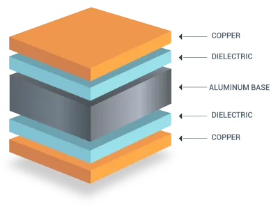
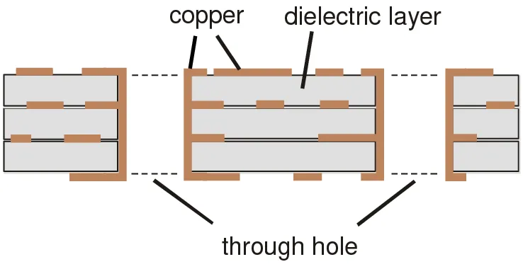
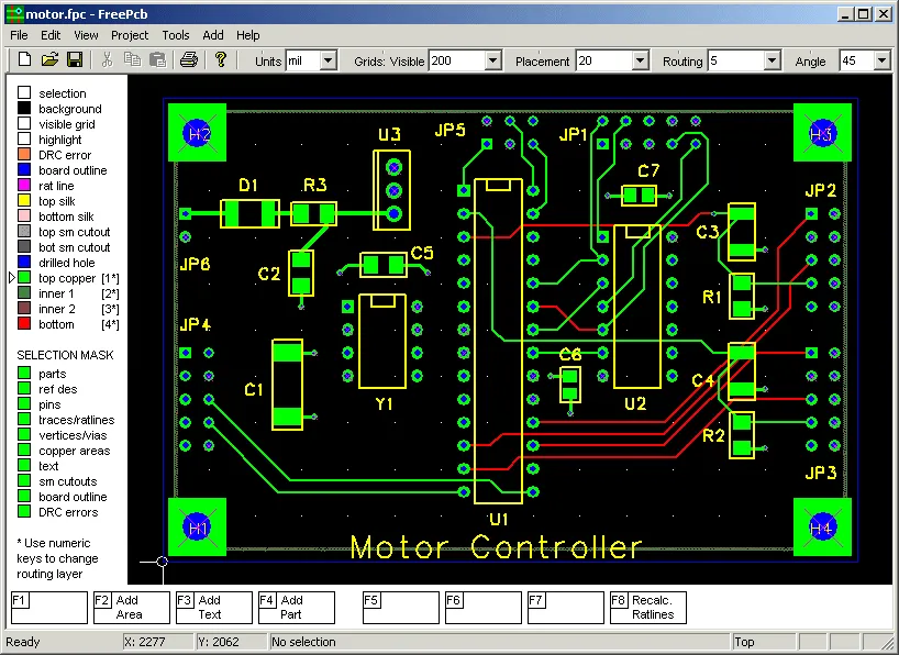
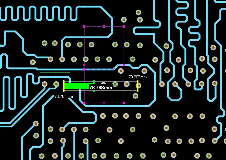
Transition from schematic to layout by placing components on a virtual board outline. Decide on single-sided or double-sided based on complexity; the single-sided PCB process suits most beginner projects due to its simplicity. Assign copper layers, route traces with appropriate widths for current, and add silkscreen for labels. Maintain minimum clearances to avoid shorts, typically guided by basic design rules. Generate drill files and Gerber outputs, which define the manufacturing layers. Review the 3D preview to visualize the final board.
Preparing Gerber Files for Home Fabrication
Gerber files are industry-standard outputs containing artwork for each layer: copper, solder mask, and silkscreen. Export them with correct apertures and units to match your fabrication method. For PCB fabrication at home, ensure files support single-sided processes by including only top-layer data. Validate files using free online viewers to confirm no export errors. These files act as your blueprint, translating design into etchable patterns. Proper preparation prevents wasted materials during etching.
Step 3: Materials and Setup for Home Fabrication
Gather copper-clad boards, photoresist film or dry film, developer solution, etchant, and safety gear for safe PCB fabrication at home. Single-sided boards use laminate with copper on one side, ideal for simple circuits. Clean the board thoroughly to remove oils, ensuring good adhesion. Set up in a well-ventilated area with gloves and goggles to handle chemicals responsibly. Organize tools like UV lamps or laser printers for pattern transfer. This preparation stage minimizes risks and sets up success.
The Single-Sided PCB Process Explained
The single-sided PCB process involves patterning one copper layer without vias, perfect for low-density designs. Apply photoresist evenly, expose to UV light through a printed transparency of your inverted Gerber image, and develop to reveal the pattern. Etch away unprotected copper, then strip remaining resist. This method avoids alignment issues of multi-layer boards. Hobbyists appreciate its low cost and straightforward workflow. Adhering to cleanliness standards ensures sharp traces.
Step 4: DIY PCB Etching Techniques
DIY PCB etching removes unwanted copper using ferric chloride or similar etchants after pattern transfer. Immerse the developed board in etchant solution at room temperature, agitating gently for uniform etching. Monitor progress every few minutes to avoid over-etching, which thins traces. Rinse immediately with water, then neutralize with baking soda solution. Dry thoroughly before inspection. This hands-on step is the heart of home fabrication, yielding professional-looking results with practice.
Toner Transfer Method for Patterning
An alternative to photoresist, toner transfer uses laser-printed layouts on glossy paper, ironed onto the copper clad. Heat transfers toner as a resist mask, which withstands etchant. Scrape off paper after cooling, touch up pinholes with marker, then etch as usual. This method excels for quick prototypes without darkroom setup. Refine technique by adjusting iron temperature and paper type. It streamlines the single-sided PCB process for hobbyists.
Advanced Tips for Clean Etching
Bubble agitation speeds etching by preventing stagnant areas, achieving uniform results faster. Control etchant temperature below 50 degrees Celsius to preserve fine features. Dispose of spent etchant responsibly per local regulations. Post-etch, inspect under magnification for bridges or pits, repairing with knife or sandpaper. These practices elevate DIY PCB etching from trial-and-error to repeatable success. Patience here pays off in reliable boards.
Step 5: Drilling Holes and Finishing
Drill vias and pad holes using a precision press drill with carbide bits sized to your design. Secure the board in a vise to prevent movement, starting with smaller bits if needed. Deburr holes with a countersink tool for smooth component insertion. Apply solder mask if desired by painting or using dry film, though many hobbyists skip for prototypes. Bake or air-dry to cure. Finishing touches like edge beveling improve handling.
Quality Checks During Manufacturing
Inspect traces for continuity with a multimeter, checking resistance between nets. Visual checks under light reveal defects like undercuts. Reference IPC-A-600 acceptability criteria for visual standards, such as allowable pitting or edge roughness. Measure trace widths with calipers to confirm design integrity. These steps catch issues early, saving rework. Consistent checks build quality into your process.
Step 6: Basic Assembly for Finished Boards
Populate the board starting with low-profile components, soldering from one side. Use flux for clean joints, heating pads briefly to avoid lifting traces. Trim leads close to the board for neatness. For surface-mount, practice with a hot air station or reflow oven setup. Test the assembled board with power applied gradually. This completes the journey from schematic to functional device.
Best Practices for Reliable Home-Made PCBs
Always wear protective gear and work in ventilated spaces during chemical steps. Start with larger trace widths for beginners to tolerate etching variations. Document each project with photos and notes for iteration. Scale up gradually from single-sided to doubles as skills grow. Store materials properly to maintain efficacy. Following J-STD-020 guidelines for handling sensitivity prevents warpage issues post-fabrication.
Common Troubleshooting for Beginners
If etching fails to produce sharp traces, check exposure time or developer strength. Blurry transfers in toner method often stem from insufficient heat or wrong paper. Drill breakage results from dull bits or misalignment; use lubricant and steady pressure. Over-etched boards show thin lines; dilute etchant or reduce time next round. Solder joints that crack indicate poor fluxing; clean and reapply. Systematic fixes turn setbacks into learning opportunities.
Conclusion
The PCB manufacturing process, from schematic to finished board, demystifies electronics for hobbyists. Techniques like DIY PCB etching and the single-sided PCB process make professional results achievable at home. With easy PCB design software and a PCB prototyping guide mindset, you iterate faster and deeper into projects. Key to success lies in preparation, safety, and iterative practice. Standards like IPC-A-600 ensure your boards meet basic quality benchmarks. Start small, and soon you will craft complex circuits confidently.
FAQs
Q1: What is DIY PCB etching, and why try it at home?
A1: DIY PCB etching involves using chemicals like ferric chloride to remove excess copper after masking traces. It suits hobbyists for quick prototypes without shipping delays. The process takes 30-60 minutes per board, building skills in pattern transfer and quality control. Start with single-sided designs to master basics before advancing. This hands-on method fosters deeper circuit understanding.
Q2: How does PCB fabrication at home compare to professional services?
A2: PCB fabrication at home excels for low-volume, custom tweaks using simple tools and etchant. Professionals handle high-density boards with automated lines, but home methods suffice for hobbyist projects. Costs drop to pennies per square inch, though turnaround is immediate. Focus on single-sided PCB process for reliability. Safety and cleanup are key trade-offs.
Q3: What makes the single-sided PCB process ideal for beginners?
A3: The single-sided PCB process limits patterning to one copper layer, simplifying alignment and etching. No vias mean fewer drills and errors, perfect for basic circuits like amplifiers. It supports DIY workflows with toner or photoresist. Results match hobby needs without multi-layer complexity. Practice yields clean boards ready for assembly.
Q4: Which easy PCB design software should hobbyists use for prototyping?
A4: Easy PCB design software features intuitive schematics, auto-routing, and Gerber export for beginners. Prioritize free tools with large libraries and 3D views for verification. They guide through PCB prototyping guide steps seamlessly. Tutorials accelerate learning curves. Export checks ensure home fabrication compatibility.
References
IPC-A-600K — Acceptability of Printed Boards. IPC, 2020
J-STD-020E — Moisture/Reflow Sensitivity Classification. JEDEC, 2014
IPC-6012E — Qualification and Performance Specification for Rigid Printed Boards. IPC, 2017