Introduction
Printed Circuit Board (PCB) manufacturing is a complex process where precision and efficiency are critical to delivering high-quality products. However, material waste during production remains a significant challenge, impacting both costs and environmental sustainability. PCB material waste cost can escalate quickly due to scrap from defective boards, inefficient layouts, or improper handling. For electric engineers and manufacturing teams, addressing PCB scrap reduction and boosting PCB manufacturing efficiency are essential to maintaining competitiveness. Adopting sustainable PCB practices and eco-friendly PCB approaches also aligns with global environmental goals. This article explores the causes of material spoilage in PCB production, outlines practical strategies for minimizing waste, and emphasizes the importance of sustainable methods to ensure long-term industry viability.
Why PCB Material Waste Matters
Material waste in PCB manufacturing directly influences operational costs and environmental impact. The production process involves expensive raw materials like copper-clad laminates, solder masks, and substrates, which contribute to high PCB material waste cost when discarded as scrap. Beyond financial implications, excessive waste poses environmental risks due to hazardous chemicals and non-biodegradable components in PCBs. For electric engineers, reducing PCB scrap is not just about cost savings but also about aligning with regulations like those outlined in industry standards. Efficient waste management enhances PCB manufacturing efficiency and supports the development of sustainable PCB practices. Addressing this issue is vital for minimizing resource depletion and fostering eco-friendly PCB production in a highly competitive industry.
Causes of PCB Material Waste in Manufacturing
Understanding the root causes of material spoilage is the first step toward effective waste reduction. Several factors contribute to PCB scrap during manufacturing, often linked to design, process, and handling issues.
Design Inefficiencies
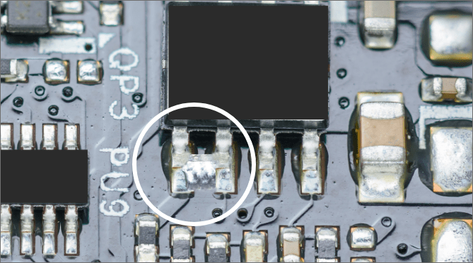
Poor PCB layout design can lead to significant material waste. When panel utilization is not optimized, large portions of the substrate remain unused, increasing scrap rates. Designs that do not account for manufacturing constraints, such as minimum trace widths or spacing, often result in defective boards that must be discarded. Engineers must prioritize design for manufacturability to ensure efficient use of materials and minimize PCB material waste cost.
Related Reading: Ways to Reduce PCB Manufacturing Costs
Process Variations
Variations in manufacturing processes, such as inconsistent etching or drilling, can cause defects that render boards unusable. Over-etching may remove excessive copper, while misaligned drilling can damage critical areas. These errors contribute to higher scrap rates and lower PCB manufacturing efficiency. Maintaining strict process controls, aligned with standards like IPC-6012E, is crucial to reducing such waste.
Material Handling Issues
Improper storage or handling of raw materials can lead to physical damage or contamination. For instance, exposure to moisture can degrade substrates, making them unsuitable for production. Mishandling during transport or assembly often results in scratches or cracks, further increasing PCB scrap. Implementing proper handling protocols is essential for preserving material integrity.
Equipment Malfunctions
Outdated or poorly maintained equipment can introduce errors in the manufacturing process. For example, miscalibrated machines may produce boards with incorrect dimensions or incomplete circuits. Regular maintenance and calibration, as recommended by industry guidelines, help prevent such issues and support PCB scrap reduction.
Practical Strategies for Minimizing PCB Material Waste
Reducing spoilage in PCB manufacturing requires a combination of design optimization, process improvements, and sustainable practices. Below are actionable strategies for electric engineers and production teams to enhance PCB manufacturing efficiency and lower PCB material waste cost.
Optimize PCB Design for Material Efficiency
Efficient design practices are fundamental to PCB scrap reduction. Utilizing panelization techniques maximizes the number of boards per panel, minimizing unused material. Software tools that simulate manufacturing outcomes can identify potential waste areas before production begins. Engineers should adhere to design guidelines, such as those in IPC-A-600K, to ensure manufacturability and reduce errors. Prioritizing modular designs also allows for easier repairs, extending board lifespan and supporting sustainable PCB goals.
Related Reading: PCB Panel Size Calculation: Enhancing Manufacturing Efficiency and Reducing Material Waste
Implement Strict Process Controls
Consistency in manufacturing processes is key to reducing defects. Establishing standardized procedures for etching, drilling, and lamination helps maintain quality. Real-time monitoring systems can detect deviations early, preventing defective batches. Compliance with standards like IPC-6012E ensures that process parameters meet industry benchmarks, directly contributing to PCB manufacturing efficiency. Regular training for operators further minimizes human error during production stages.
Enhance Material Handling Practices
Proper storage conditions, such as controlled humidity and temperature, preserve raw material quality. Using protective packaging during transport prevents physical damage. Clear labeling and organized inventory systems reduce the risk of using expired or incorrect materials. These practices not only lower PCB scrap but also align with eco-friendly PCB principles by extending material usability.
Adopt Advanced Manufacturing Technologies
Investing in modern equipment with precision capabilities reduces errors and material waste. Automated systems for cutting and drilling improve accuracy, while advanced imaging technologies detect defects before further processing. These innovations enhance PCB manufacturing efficiency and support sustainable PCB production by minimizing resource consumption. Regular equipment audits ensure consistent performance and adherence to technical standards.
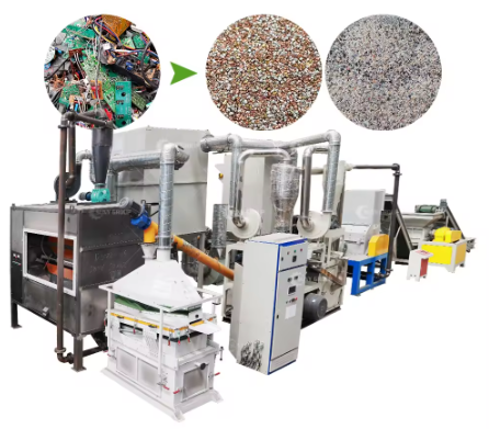
Recycle and Reuse Scrap Materials
Where possible, scrap materials like copper and substrates should be recycled. Processes that recover valuable metals from defective boards can offset PCB material waste cost. Implementing a circular approach, where waste is repurposed into new production cycles, fosters eco-friendly PCB practices. Engineers should collaborate with recycling experts to ensure compliance with environmental regulations during material recovery.
Sustainable Practices for Eco-Friendly PCB Production
Sustainability in PCB manufacturing goes beyond waste reduction. It involves adopting practices that minimize environmental impact while maintaining production efficiency. Electric engineers play a crucial role in driving sustainable PCB initiatives through informed material choices and process innovations.
Use of Environmentally Friendly Materials
Selecting substrates and coatings with lower environmental impact is a step toward eco-friendly PCB production. Materials that comply with restrictions on hazardous substances, as outlined in relevant standards, reduce toxicity in waste. Biodegradable or recyclable options, where feasible, further support sustainable PCB goals. Engineers should evaluate material properties to balance performance with environmental considerations.
Energy-Efficient Manufacturing Processes
Reducing energy consumption during production lowers the overall carbon footprint. Optimizing machine settings for minimal power usage and scheduling production runs to avoid idle times are effective strategies. Energy audits, aligned with guidelines like ISO 50001:2018, provide insights into areas for improvement. These efforts contribute to PCB manufacturing efficiency and align with eco-friendly PCB objectives.
Waste Management Systems
Implementing structured waste management systems ensures proper disposal and recycling of scrap. Segregating hazardous and non-hazardous waste prevents contamination and facilitates recovery. Adhering to environmental management standards, such as ISO 14001:2015, helps establish protocols for handling PCB scrap. These systems are essential for minimizing PCB material waste cost and promoting sustainable practices.
Insights for Electric Engineers on Waste Reduction
For electric engineers, minimizing PCB material waste requires a proactive approach across design and collaboration with manufacturing teams. Conducting thorough design reviews before production can identify potential waste sources. Working closely with process engineers ensures that designs are practical and aligned with production capabilities. Additionally, staying updated on industry standards, such as IPC-A-600K, provides a framework for quality and efficiency. By integrating waste reduction into every stage of the PCB lifecycle, engineers can significantly impact both cost savings and environmental sustainability.
Conclusion
PCB material waste remains a critical concern in manufacturing, affecting both operational costs and environmental sustainability. By understanding the causes of spoilage, such as design inefficiencies and process variations, electric engineers can implement targeted strategies for PCB scrap reduction. Optimizing designs, enforcing strict process controls, and adopting sustainable practices contribute to higher PCB manufacturing efficiency and lower PCB material waste cost. Embracing eco-friendly PCB approaches, from material selection to recycling, ensures long-term industry viability. Through consistent efforts, the PCB sector can achieve a balance between quality production and responsible resource management.
FAQs
Q1: How does PCB material waste cost impact overall manufacturing budgets?
A1: PCB material waste cost can significantly strain budgets due to the high price of raw materials like copper-clad laminates. Scrap from defective boards or inefficient designs directly increases expenses. By focusing on waste reduction strategies, such as optimized panelization and process controls, manufacturers can save resources. Aligning with industry standards ensures efficiency, ultimately reducing financial losses in production.
Q2: What are key methods for achieving PCB scrap reduction in production?
A2: PCB scrap reduction relies on optimized design, strict process monitoring, and proper material handling. Efficient panel layouts minimize unused substrates, while consistent manufacturing parameters prevent defects. Storing materials in controlled environments avoids damage. Adhering to standards like IPC-6012E helps maintain quality, ensuring fewer boards are discarded during production stages.
Q3: How can sustainable PCB practices benefit the environment?
A3: Sustainable PCB practices reduce environmental impact by minimizing waste and using eco-friendly materials. Recycling scrap and selecting less toxic substrates lower pollution risks. Energy-efficient processes cut carbon emissions during manufacturing. Following frameworks like ISO 14001:2015 supports responsible waste management, preserving resources and aligning the industry with global environmental goals.
Q4: What role does PCB manufacturing efficiency play in waste reduction?
A4: PCB manufacturing efficiency is crucial for reducing waste by ensuring processes are streamlined and error-free. Consistent etching, drilling, and lamination prevent defective boards. Real-time monitoring detects issues early, avoiding large scrap batches. Efficient systems, guided by standards like IPC-A-600K, optimize resource use, directly lowering material spoilage and production costs.
References
IPC-6012E — Qualification and Performance Specification for Rigid Printed Boards. IPC, 2020.
IPC-A-600K — Acceptability of Printed Boards. IPC, 2020.
ISO 14001:2015 — Environmental Management Systems. ISO, 2015.
ISO 50001:2018 — Energy Management Systems. ISO, 2018.


