Introduction
High-density interconnect (HDI) printed circuit boards represent a cornerstone of modern electronics, enabling compact devices with enhanced signal integrity and higher component density. Microvias, essential to HDI designs, allow connections between adjacent layers without penetrating the entire board stackup, thus saving space and improving electrical performance. However, the PCB microvia cost can escalate quickly due to specialized manufacturing processes required for these small features, typically defined as vias with diameters of 150 micrometers or less. Engineers must navigate HDI PCB cost drivers such as material selection, via configuration, and process complexity to achieve viable production economics. Balancing these elements ensures that high-performance designs remain affordable without compromising reliability. This analysis delves into microvia manufacturing costs, key influencing factors, and proven optimization techniques drawn from factory perspectives.
Microvias facilitate finer line widths and spaces, supporting advanced packaging like ball grid arrays with pitches below 0.5 mm. Yet, their implementation demands precision laser drilling, electroplating, and often via filling, each step adding to the overall expense. Factory experience shows that poor design choices amplify these costs through lower yields and rework. Understanding these dynamics empowers electrical engineers to make informed decisions during the design phase. As HDI adoption grows in sectors like telecommunications and consumer electronics, mastering PCB microvia cost management becomes critical for project success.
What Are Microvias and Why Do They Matter in HDI Manufacturing?
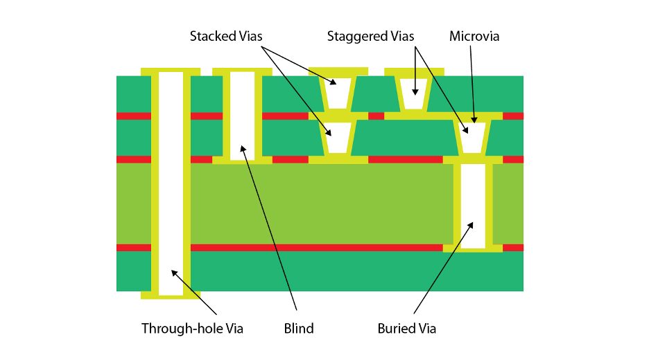
Microvias are laser-drilled interconnects with apertures under 150 micrometers, distinguishing them from standard through-holes that exceed this size. In HDI PCBs, they form blind or buried vias, connecting only specific layers to maximize routing density. Industry standards like IPC-2226 classify HDI boards by microvia buildup, such as 1-N-1 for any-layer configurations with one microvia layer per side. These structures matter because they enable smaller form factors while maintaining signal integrity, crucial for high-speed applications. However, their small size heightens sensitivity to thermal and mechanical stresses during fabrication and assembly.
The relevance of microvias extends to cost implications, as HDI PCB cost drivers stem directly from their integration. Factories observe that microvia density correlates strongly with production cycle time, influencing throughput and pricing. Without microvias, achieving equivalent density would require more layers or larger boards, often proving more expensive in materials alone. Engineers benefit from recognizing how microvia types - staggered, stacked, or filled - affect both performance and manufacturability. Proper application reduces overall board size, potentially offsetting higher per-via costs through economies in substrate usage.
Staggered microvias offset positions across layers to simplify plating, while stacked ones align directly, demanding tighter tolerances. Each choice impacts reliability under IPC-6016 guidelines for HDI qualification. Ignoring these distinctions leads to inflated microvia manufacturing costs from yield losses. Thus, microvias not only drive innovation but also necessitate strategic cost planning in HDI workflows.
Key HDI PCB Cost Drivers in Microvia Manufacturing
Material selection tops the list of HDI PCB cost drivers, particularly resin systems optimized for laser drilling. Low-loss dielectrics with uniform ablation properties prevent residue buildup, but they command premium pricing over standard FR-4. Buildup foils and photoresists tailored for fine features add further expense, as do copper foils with low roughness for high-frequency performance. Factories track these inputs closely, as material waste rises with microvia density due to precise panel utilization requirements.
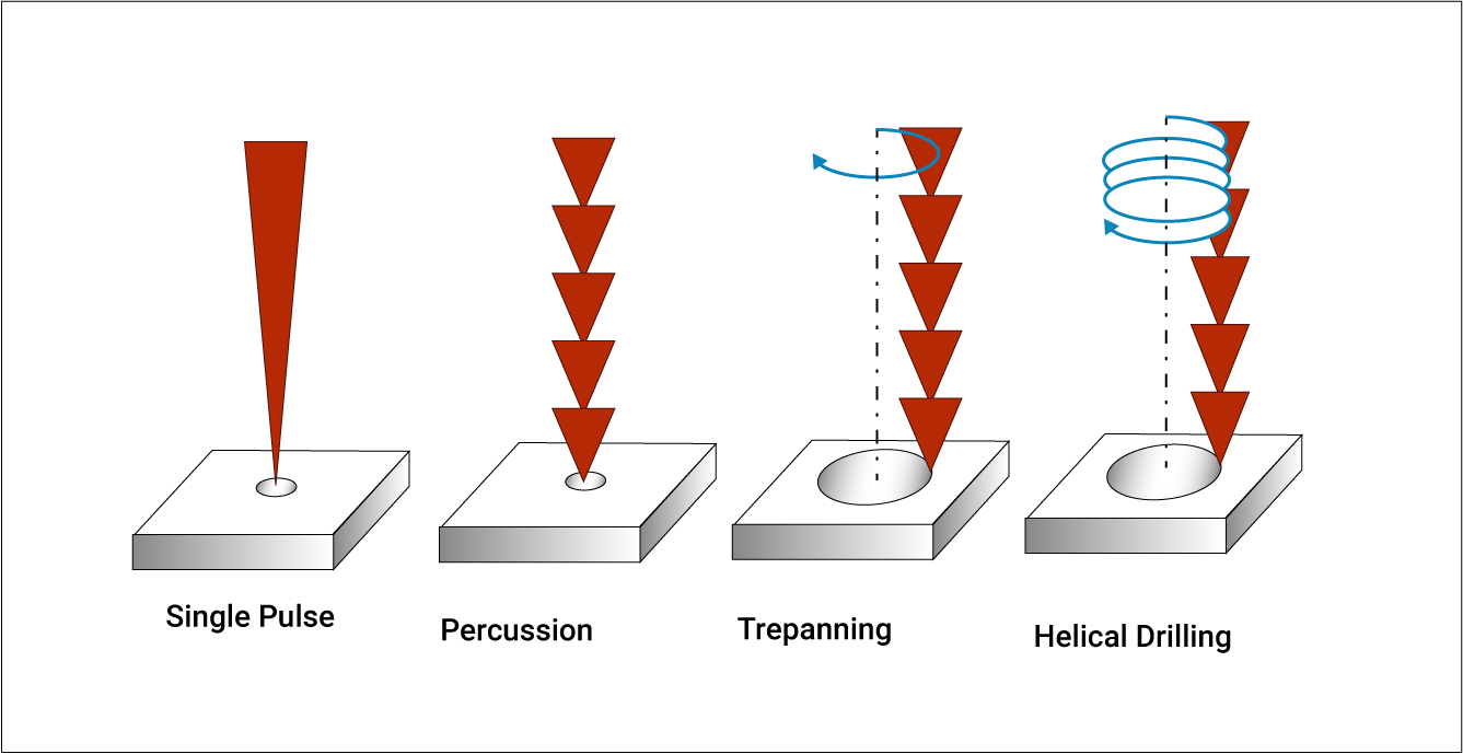
Process complexity follows, with sequential lamination cycles multiplying for multi-order HDI builds like 2-N-4 or 3-N-4. Each cycle involves lamination, drilling, desmear, plating, and inspection, extending lead times and equipment depreciation. Laser drilling dominates for microvias, employing UV or CO2 types based on dielectric thickness; UV excels for thinner layers but requires multiple passes for deeper vias, hiking operational costs. Electroplating blind vias demands controlled copper deposition to avoid voids, a step prone to defects that necessitate scrap.
Yield rates represent a hidden yet substantial cost factor in microvia manufacturing. Smaller apertures increase drill breakout risks and plating inconsistencies, per IPC acceptance criteria. Factories mitigate this through process controls, but high microvia counts still elevate defect densities, triggering 100% electrical testing. Board size and layer count amplify these effects, as larger panels spread fixed setup costs but heighten warpage risks during buildup.
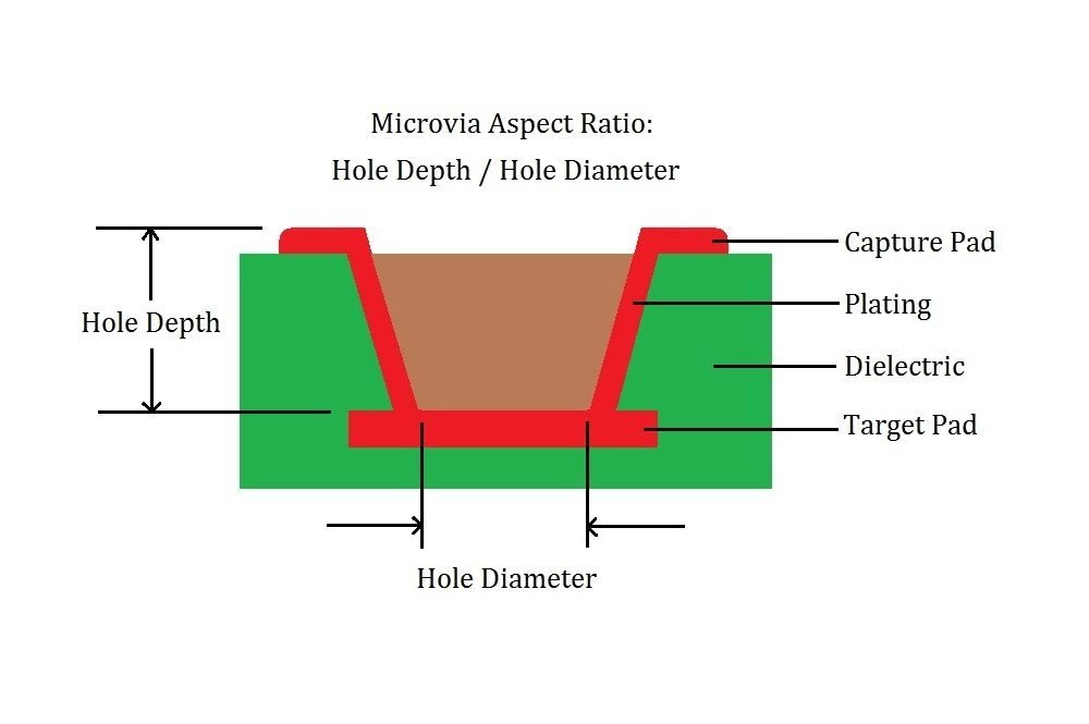
Via configuration further influences costs: filled microvias, using conductive epoxy or electroplated copper, enable via-in-pad designs but require additional filling and planarization steps. Unfilled options suffice for simpler stacks, trimming expenses. Aspect ratios, capped at 1:1 by design standards, limit depth but still challenge plating uniformity in stacked arrays. Engineers optimizing for staggered configurations often see 20-30% lower process steps compared to stacked, based on factory lamination cycles.
Microvia Manufacturing Processes and Cost Implications
Fabrication begins with core preparation, followed by buildup layers where microvias form. Sequential buildup (SBU) processes drill vias post-lamination using excimer or CO2 lasers, which ablate dielectrics selectively without damaging copper. Desmear via plasma or permanganate removes residue, ensuring plating adhesion; inadequate cleaning leads to reliability failures and rework costs. Electroplating then deposits copper, with pulse reverse techniques controlling thickness for high aspect ratios.
Filling processes vary: conductive paste suits low-cost prototypes, while full copper electrofill supports high-current paths but demands longer plating baths. Planarization via grinding or etching follows to restore flatness for outer layers. Each HDI order increments these steps, as inner microvias must survive outer processing. Factories emphasize tooling longevity, as microvia drills wear faster, necessitating frequent replacements.
Inspection integrates throughout, with automated optical systems verifying via geometry and continuity. Cross-sectioning samples per IPC-6016 confirms barrel quality, though sampling limits scalability. Thermal cycling simulates assembly stresses, exposing weak points early. These controls safeguard yield but add to microvia manufacturing cost, particularly for high-volume runs.
Environmental factors like cleanroom maintenance and waste handling for etchants contribute indirectly. Energy-intensive lasers and plating lines scale with production, favoring larger panels. Engineers designing within process windows minimize these burdens, aligning with factory capabilities for cost predictability.
Microvia Design Optimization for Reducing Microvia Cost
Optimizing microvia placement starts with minimizing count through efficient routing. Tools simulate fanout from fine-pitch BGAs, favoring dog-bone escapes over direct vias where possible. Staggered arrays reduce buildup cycles versus stacked, preserving density while cutting lamination steps. Larger apertures near 150 micrometers ease drilling and plating, boosting yield without sacrificing much space.
Stackup planning integrates microvias thoughtfully: outer layers for high-speed signals, inner for power. Aspect ratio adherence to 1:1 prevents plating voids, a common failure mode. Via-in-pad with filled microvias enables tighter layouts, amortizing fill costs over denser routing. Factories recommend tear-drops at pads to distribute stress, enhancing reliability per IPC-2226.
Material synergies lower costs: select drillable resins matching laser wavelengths, reducing passes. Simulate warpage from CTE mismatches to avoid yield killers. Panel-level design maximizes utilization, spreading NRE across units.
Process collaboration with fabricators refines designs pre-tapeout. DFM reviews flag high-risk clusters, suggesting alternatives like embedded components. These steps collectively drive down PCB microvia cost by 15-25% in practice, balancing performance needs.
Practical Insights from HDI Factory Production
Factory data highlights stacked microvias suiting ultra-dense apps but at double the buildup cost of staggered. A typical 1-N-1 board uses staggered for cost-effectiveness, transitioning to stacked only for escape routing limits. Yield mapping reveals outer microvias tolerate looser specs, reserving tight tolerances inwardly.
Troubleshooting focuses on plating defects: voids trace to desmear issues, resolved via optimized chemistries. Thermal reliability testing per JEDEC standards uncovers electromigration risks in filled vias, guiding fill choices. Engineers applying these insights achieve first-pass success, minimizing iterations.
Conclusion
PCB microvia cost hinges on interplay of design, materials, and processes in HDI manufacturing. Key drivers like via type, buildup order, and yield demand careful management to balance affordability with performance. Strategies such as staggered configurations, optimized stackups, and DFM collaboration effectively reduce microvia manufacturing cost. Adhering to standards like IPC-2226 and IPC-6016 ensures reliability amid cost pressures. Electrical engineers equipped with these factory-aligned insights can deliver high-density boards that meet market demands efficiently. Prioritizing microvia design optimization unlocks HDI potential without excessive expense.
FAQs
Q1: What are the main HDI PCB cost drivers related to microvias?
A1: HDI PCB cost drivers include sequential lamination cycles, laser drilling precision, and via filling methods. Stacked microvias increase buildup steps compared to staggered, elevating expenses. Material choices for laser-drillable dielectrics and yield impacts from small apertures further influence pricing. Factory controls mitigate these through process optimization.
Q2: How does microvia design optimization reduce PCB microvia cost?
A2: Microvia design optimization reduces PCB microvia cost by minimizing via counts, using larger feasible apertures, and preferring staggered over stacked structures. Efficient stackups and via-in-pad techniques cut lamination cycles. Collaborating on DFM ensures manufacturability, boosting yields and trimming rework.
Q3: What role do manufacturing processes play in microvia manufacturing cost?
A3: Microvia manufacturing cost rises with laser drilling passes, electroplating uniformity, and filling requirements. UV lasers suit thin dielectrics but demand multiple hits for depth, while desmear and inspection add steps. Optimizing for 1:1 aspect ratios per standards lowers defect risks and cycle times.
Q4: Can staggered microvias always replace stacked for cost savings in HDI?
A4: Staggered microvias offer cost savings in HDI by simplifying plating and reducing laminations, ideal for moderate densities. Stacked excel in ultra-tight routing but at higher microvia manufacturing cost due to alignment challenges. Selection depends on BGA pitch and layer transitions, guided by IPC-2226.
References
IPC-2226A - Sectional Design Standard for High Density Interconnect (HDI) Printed Boards. IPC, 2003
IPC-6016D - Qualification and Performance Specification for High Density Interconnect (HDI) Printed Boards. IPC, 2015
JEDEC J-STD-020E - Moisture/Reflow Sensitivity Classification for Nonhermetic Surface Mount Devices. JEDEC, 2014


