Introduction
Designing a printed circuit board (PCB) prototype is a critical step in electronics development. For electrical engineers, ensuring that a design aligns with manufacturability principles can prevent costly errors and multiple re-spins. PCB design for manufacturability (DFM) focuses on creating layouts that are efficient to produce while maintaining functionality and reliability. Ignoring PCB DFM guidelines often leads to production delays, increased costs, and performance issues. This article explores essential design for manufacturability practices, highlights common PCB prototype errors, and offers practical strategies to avoid PCB re-spins. By following established PCB design rules, engineers can streamline the transition from prototype to production, saving time and resources in the process. Let’s dive into the core concepts and actionable steps for effective PCB prototype design.
What Is PCB Design for Manufacturability (DFM) and Why It Matters
PCB design for manufacturability refers to the practice of designing circuit boards with manufacturing constraints and processes in mind. It ensures that a PCB can be produced efficiently, reliably, and at scale without compromising quality. For electrical engineers, adhering to PCB DFM guidelines is vital because early design decisions directly impact production costs and timelines. A design that overlooks manufacturability may result in fabrication challenges, assembly failures, or the need for costly re-spins.
The importance of DFM lies in its ability to bridge the gap between theoretical design and practical production. By considering factors like component placement, trace routing, and material selection during the PCB prototype manufacturing phase, engineers can minimize errors. This approach reduces the risk of delays and ensures that the final product meets performance expectations. Ultimately, integrating PCB design rules early saves resources and enhances project outcomes.
Technical Principles of PCB DFM
Understanding the technical foundations of PCB design for manufacturability is essential for creating error-free prototypes. Several key principles guide this process, each addressing specific aspects of production readiness.
Component Placement and Spacing
Proper component placement is a cornerstone of DFM. Components must be positioned to avoid interference during assembly and to facilitate efficient routing. Overcrowding can lead to soldering issues or thermal problems. Adhering to spacing guidelines as outlined in standards like IPC-7351B ensures accessibility for manufacturing equipment and reduces the risk of defects.
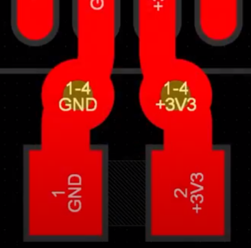
Trace Width and Clearance
Trace width and clearance directly affect electrical performance and manufacturability. Narrow traces may not handle current loads, while insufficient clearance can cause short circuits. Following PCB design rules from standards such as IPC-2221B helps maintain appropriate dimensions for signal integrity and production feasibility. This prevents issues during etching or soldering processes.
Via and Drill Hole Specifications
Vias and drill holes must meet large pcb manufacturer capabilities to avoid fabrication errors. Oversized or undersized holes can weaken the board or complicate assembly. Standards like IPC-6012E provide specifications for via sizes and tolerances, ensuring compatibility with drilling and plating processes. Respecting these limits during prototype design minimizes production hiccups.
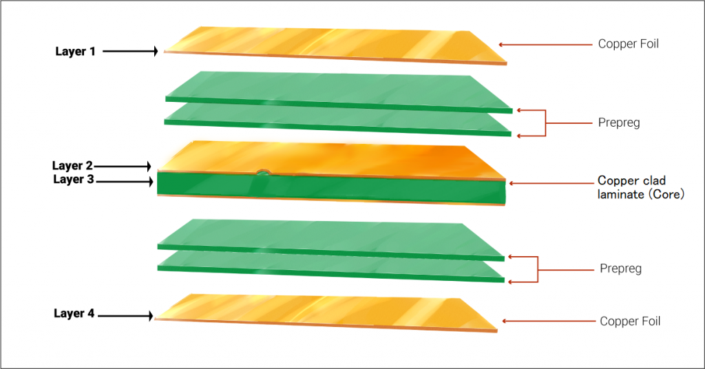
Material and Layer Stackup Considerations
Selecting suitable materials and planning the layer stackup are critical for DFM. Material properties influence thermal management and signal performance, while stackup design impacts impedance control. Referencing guidelines from IPC-4101E for material selection ensures that the chosen substrates align with manufacturing constraints. A well-planned stackup also prevents warpage or delamination during production.
Common PCB Prototype Errors and Their Impact
PCB prototype errors often stem from overlooking DFM principles. These mistakes can lead to significant setbacks, including the need for re-spins. Below are frequent issues encountered by electrical engineers.
- Inadequate Clearance: Insufficient spacing between traces or components can cause electrical shorts or assembly challenges. This often requires redesign, increasing costs.
- Incorrect Footprints: Mismatched component footprints lead to soldering failures or misaligned parts. Verifying footprints against standards like IPC-7351B prevents such errors.
- Poor Thermal Management: Failing to account for heat dissipation can result in component damage. Incorporating thermal vias or heat sinks early avoids performance issues.
- Unrealistic Tolerances: Specifying tolerances beyond manufacturing capabilities leads to rejected boards. Aligning designs with IPC-6012E ensures feasible production.
These errors highlight the importance of integrating PCB DFM guidelines from the start. Addressing them during the prototype phase saves time and prevents costly re-spins.
Practical Solutions and Best Practices for PCB DFM
To avoid PCB prototype errors and ensure manufacturability, electrical engineers can adopt several best practices. These actionable strategies align with industry standards and facilitate a smooth transition to production.
Follow Standardized Design Rules
Adhering to established PCB design rules is the foundation of DFM. Standards like IPC-A-600K provide criteria for acceptable board quality, while IPC-2221B offers guidance on trace and clearance specifications. Using these as a reference during design minimizes errors and ensures compatibility with manufacturing processes.
Use Design Rule Checks (DRC)
Implementing design rule checks within PCB design software helps identify potential issues before fabrication. DRC tools flag violations in spacing, trace width, or via placement, allowing engineers to correct errors early. Aligning DRC settings with standards like IPC-6012E ensures accuracy and reduces the likelihood of re-spins.
Optimize Component Placement
Place components logically to simplify routing and assembly. Group related components together and maintain adequate spacing for soldering equipment. Referencing IPC-7351B for land pattern standards ensures footprints are compatible with automated assembly processes. This approach enhances efficiency and reduces manufacturing defects.
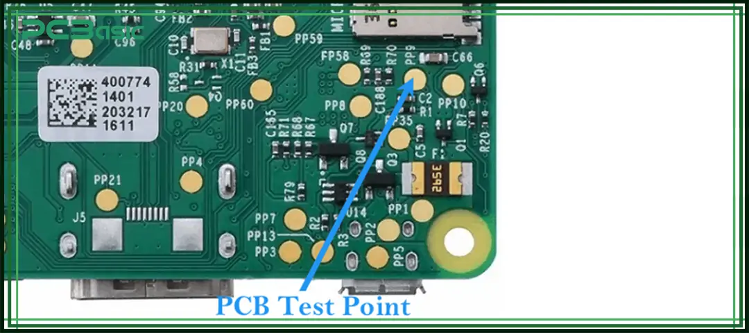
Plan for Testability
Incorporate test points and access areas in the design to facilitate quality checks during production. Standards like IPC-9252A outline guidelines for testability, ensuring that critical nodes are accessible. Planning for testability during the prototype stage prevents delays in validation and debugging.
Collaborate with Fabrication Teams
Engaging with manufacturing teams early provides insights into their capabilities and limitations. Discussing aspects like minimum trace width or via sizes ensures the design aligns with production constraints. While specific tools or companies are not referenced here, following general guidelines from IPC-6012E helps standardize communication with fabricators.
Account for Material and Environmental Factors
Select materials that match the application’s thermal and mechanical requirements. Standards such as IPC-4101E provide specifications for laminate properties, aiding in informed decisions. Additionally, consider environmental factors like humidity or temperature during design to prevent issues like warpage or delamination in production.
Troubleshooting Insight: Identifying DFM Issues in Prototypes
Even with careful planning, DFM issues may arise during PCB prototype testing. Electrical engineers can use a systematic approach to troubleshoot and resolve these problems. Start by reviewing the design against PCB DFM guidelines, focusing on spacing, footprints, and via specifications. If assembly errors occur, inspect component placement and soldering quality, ensuring compliance with IPC-7351B standards. For electrical failures, check trace widths and clearances using IPC-2221B as a benchmark. Documenting findings and iterating the design based on test results helps avoid similar issues in future revisions. This methodical process reduces the risk of re-spins and ensures manufacturability.
Conclusion
Designing a PCB prototype with manufacturability in mind is crucial for electrical engineers aiming to avoid costly errors. By adhering to PCB DFM guidelines and following established PCB design rules, engineers can minimize prototype errors and prevent the need for re-spins. Key practices include optimizing component placement, ensuring proper trace clearances, and aligning designs with industry standards like IPC-6012E and IPC-2221B. Early consideration of manufacturing constraints saves time, reduces costs, and ensures a seamless transition to full-scale production. Implementing these strategies empowers teams to deliver reliable and efficient PCB designs consistently.
FAQs
Q1: What are the most important PCB DFM guidelines to follow during prototype design?
A1: Following PCB DFM guidelines ensures manufacturability. Prioritize proper component spacing, trace width, and clearance as per IPC-2221B standards. Verify footprints using IPC-7351B to avoid assembly issues. Incorporate test points for quality checks and select materials aligned with IPC-4101E. These steps reduce errors and streamline production.
Q2: How can engineers avoid PCB prototype errors in early design stages?
A2: To avoid PCB prototype errors, engineers should use design rule checks aligned with IPC-6012E standards. Ensure accurate component placement and verify tolerances. Collaborate with fabrication teams to understand constraints and test designs thoroughly. Early validation prevents costly mistakes and re-spins.
Q3: Why is design for manufacturability critical in preventing PCB re-spins?
A3: Design for manufacturability is essential to prevent PCB re-spins by aligning designs with production capabilities. Following PCB design rules like those in IPC-A-600K ensures boards are producible without defects. Addressing issues like spacing or thermal management early avoids redesigns, saving time and resources.
Q4: What role do PCB design rules play in ensuring prototype success?
A4: PCB design rules, such as those in IPC-2221B, provide a framework for creating manufacturable boards. They guide trace sizing, component placement, and via specifications, reducing errors. Adhering to these rules during prototype design ensures functionality and compatibility with assembly processes, leading to successful outcomes.
References
IPC-6012E — Qualification and Performance Specification for Rigid Printed Boards. IPC, 2020.
IPC-2221B — Generic Standard on Printed Board Design. IPC, 2012.
IPC-7351B — Generic Requirements for Surface Mount Design and Land Pattern Standard. IPC, 2010.
IPC-A-600K — Acceptability of Printed Boards. IPC, 2020.
IPC-4101E — Specification for Base Materials for Rigid and Multilayer Printed Boards. IPC, 2017.
IPC-9252A — Requirements for Electrical Testing of Unpopulated Printed Boards. IPC, 2008.


