Introduction
For electronic hobbyists, creating a printed circuit board (PCB) prototype at home is an exciting step toward bringing ideas to life. Whether you are designing a simple LED circuit or a complex microcontroller project, understanding DIY PCB prototype techniques can save time and money while offering hands-on learning. This guide explores home PCB fabrication methods, including the toner transfer method, PCB etching, and PCB drilling. It also covers simple PCB projects to help beginners build skills. With practical advice and clear steps, hobbyists can navigate the process of crafting functional boards without advanced equipment. Let’s dive into the world of PCB prototyping and uncover how to start this rewarding journey from your own workspace.
What Is PCB Prototyping and Why It Matters
PCB prototyping involves creating an initial version of a circuit board to test a design before full-scale production. For hobbyists, this process is crucial as it allows experimentation with layouts and components at a low cost. A prototype helps identify errors in design, such as incorrect traces or component placement, ensuring the final product works as intended. It also offers a chance to refine skills in soldering, etching, and drilling.
In the broader electronics field, prototyping is a fundamental step in product development. It bridges the gap between theoretical designs and practical applications. For beginners, mastering DIY PCB prototype techniques builds confidence and fosters creativity. By fabricating boards at home, hobbyists gain control over every aspect of their projects, from design to assembly, making the learning process deeply engaging.
Technical Principles of Home PCB Fabrication
Understanding PCB Basics
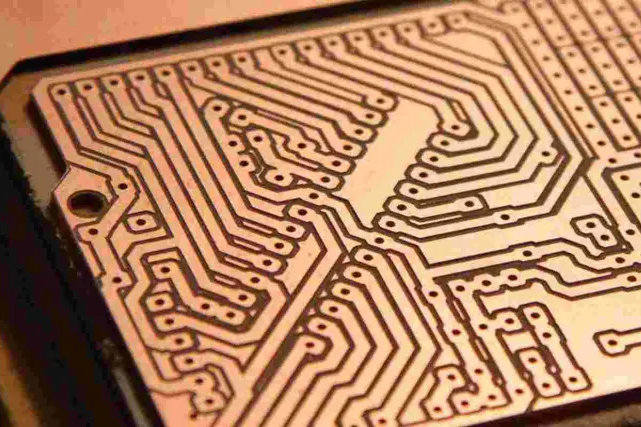
A PCB consists of a non-conductive substrate, often fiberglass, with conductive copper traces laminated on one or both sides. These traces connect electronic components to form a functional circuit. In home PCB fabrication, hobbyists replicate this structure using accessible materials and methods. The goal is to transfer a circuit design onto the board and remove excess copper to create isolated paths.
Key Methods for DIY PCB Prototyping
Several techniques are suitable for beginners looking to create a DIY PCB prototype. Each method has unique steps, tools, and challenges, but they all aim to achieve a usable circuit board.
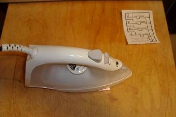
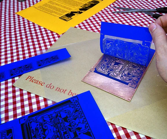
- Toner Transfer Method: This popular approach uses a laser printer to print a circuit design onto special paper. The toner acts as a resist when transferred to the copper board using heat, typically from an iron. After transfer, the board undergoes etching to remove unprotected copper.
- PCB Etching: Etching removes unwanted copper from the board using a chemical solution, such as ferric chloride or a mixture of hydrogen peroxide and hydrochloric acid. The resist, whether toner or photoresist, protects the desired traces during this process.
- PCB Drilling: Once etching is complete, holes are drilled into the board for through-hole components. A small handheld drill or a drill press with fine bits ensures precision for component leads and mounting.
These methods form the backbone of home PCB fabrication, allowing hobbyists to create functional prototypes with minimal investment.
Safety Considerations
Working with chemicals and tools requires caution. Etching solutions are corrosive and must be handled with gloves and proper ventilation. Drilling produces fine dust, so wearing a mask is advisable. Always store chemicals in labeled containers away from children and pets. Safety is a priority in every step of DIY PCB prototype creation.
Practical Solutions for Home PCB Fabrication
Step-by-Step Guide to the Toner Transfer Method
The toner transfer method is a beginner-friendly way to start with home PCB fabrication. Follow these steps for a successful transfer.
- Design your circuit using software that allows printing in mirror mode. Ensure the layout matches the board size.
- Print the design on glossy paper or transfer paper using a laser printer. Inkjet printers will not work for this method.
- Clean the copper board with steel wool or sandpaper to remove oxidation. A shiny surface ensures better toner adhesion.
- Place the printed design face down on the board. Use an iron on high heat to transfer the toner, pressing firmly for several minutes.
- Soak the board in water to remove the paper, leaving the toner on the copper. Inspect for any missing traces and correct with a permanent marker if needed.
PCB Etching at Home
After transferring the design, etching defines the circuit traces. Here’s how to proceed.
- Prepare the etching solution in a plastic container. Ferric chloride is a common choice, but always follow safety guidelines.
- Submerge the board in the solution. Agitate gently to speed up the process, which may take 10 to 30 minutes.
- Check periodically until all unprotected copper is removed. Rinse the board with water to stop the reaction.
- Remove the toner resist using acetone or rubbing alcohol to reveal the copper traces.
Ensure proper disposal of used chemicals according to local regulations. Never pour them down the drain.
PCB Drilling for Component Placement
Drilling is the final step in preparing the board for assembly. Use a drill with bits sized for your component leads, typically 0.8 to 1.2 mm. Secure the board on a stable surface to avoid slipping. Drill slowly to prevent breaking bits or damaging the board. Clean the board afterward to remove debris. Precision in PCB drilling ensures components fit correctly during assembly.
Tools and Materials for Beginners
Here’s a list of essential items for DIY PCB prototype creation.
- Copper-clad board (single or double-sided)
- Laser printer and transfer paper
- Iron or laminator for toner transfer
- Etching solution and plastic container
- Drill with small bits
- Safety gear like gloves and goggles
These tools are affordable and widely available, making home PCB fabrication accessible to all hobbyists.
Simple PCB Projects for Beginners
Starting with simple PCB projects helps build skills before tackling complex designs. Here are a few ideas to inspire beginners.
- LED Blinking Circuit: Create a board with a microcontroller to control LED blinking patterns. This project introduces basic trace routing and soldering.
- Power Supply Module: Design a small board to convert AC to DC for low-power devices. It’s a practical way to learn about rectifiers and regulators.
- Audio Amplifier: Build a circuit to amplify audio signals using a few transistors. This project teaches component placement and signal paths.
Each of these projects can be completed using the toner transfer method and basic etching. They offer a hands-on way to understand circuit functionality.
Tips for Success
Start with small boards to minimize errors. Test your design on a breadboard before committing to a PCB. Double-check the mirrored layout before printing to avoid reversed traces. Patience is key during etching and drilling, as rushing can lead to mistakes. These practices ensure better results in home PCB fabrication.
Troubleshooting Common Issues in DIY PCB Prototyping
Hobbyists often face challenges during PCB prototyping. Here are solutions to frequent problems.
- Incomplete Toner Transfer: If toner doesn’t stick properly, ensure the board is clean and increase iron heat or pressure. Test on scrap boards first.
- Over-Etching: Leaving the board in solution too long can damage traces. Monitor closely and remove once copper is gone from unmasked areas.
- Drill Misalignment: Use a punch to mark hole locations before drilling. This prevents bits from wandering off target.
Addressing these issues builds problem-solving skills essential for more advanced projects.
Conclusion
PCB prototype manufacturing at home opens up a world of possibilities for electronic hobbyists. By mastering techniques like the toner transfer method, PCB etching, and PCB drilling, beginners can create functional boards for simple PCB projects. This guide provides a foundation to start with confidence, offering step-by-step instructions and troubleshooting tips. As skills grow, hobbyists can explore more intricate designs, turning concepts into reality. Embrace the learning curve, prioritize safety, and enjoy the process of crafting your own circuits from scratch.
FAQs
Q1: What is the easiest way to start with a DIY PCB prototype at home?
A1: The toner transfer method is the simplest for beginners. Print your design with a laser printer on transfer paper, transfer it to a copper board using an iron, and etch away excess copper. It requires minimal tools and offers good results for basic projects. Always prioritize safety when handling chemicals during etching.
Q2: How can I ensure safety during PCB etching at home?
A2: Wear gloves, goggles, and work in a ventilated area when using etching solutions like ferric chloride. Store chemicals securely and dispose of them per local guidelines. Avoid skin contact and keep solutions away from children. Safety is critical in home PCB fabrication to prevent accidents.
Q3: What are some simple PCB projects for a beginner hobbyist?
A3: Start with an LED blinking circuit or a small power supply module. These projects teach basic design and soldering skills. Use the toner transfer method for trace creation and practice PCB drilling for component holes. They are achievable with basic tools and minimal experience.
Q4: Why does my toner not transfer properly during home PCB fabrication?
A4: Incomplete transfer often happens due to a dirty board or insufficient heat. Clean the copper surface thoroughly with steel wool. Apply firm pressure with a hot iron for several minutes. Test on scrap material to perfect your technique before working on the final board.
References
IPC-A-600K — Acceptability of Printed Boards. IPC, 2020.
IPC-6012E — Qualification and Performance Specification for Rigid Printed Boards. IPC, 2017.


