Introduction
High-frequency applications demand exceptional PCB quality to handle signals operating above 1 GHz, where even minor imperfections can degrade performance. Engineers designing for telecommunications, radar systems, and high-speed data processing must prioritize high-frequency PCB quality to prevent issues like signal distortion and data errors. Factors such as material properties, trace geometry, and manufacturing precision directly influence outcomes in these environments. This article explores critical aspects of signal integrity PCB design and impedance control PCB techniques from a factory perspective. By aligning with established standards, manufacturers ensure boards meet rigorous performance criteria. Understanding these elements empowers electric engineers to select and verify PCBs effectively.
Defining High-Frequency PCB Quality and Its Importance
High-frequency PCB quality refers to the ability of a printed board to maintain electrical performance under rapid signal transitions, minimizing losses and distortions. In applications like 5G infrastructure and automotive radar, poor quality leads to increased bit error rates and reduced system reliability. Factory processes must control variables such as dielectric constant consistency and surface roughness to achieve this. Signal integrity PCB becomes paramount as frequencies rise, where electromagnetic interference and propagation delays amplify. Impedance control PCB ensures predictable signal paths, preventing mismatches that cause reflections. Ultimately, quality directly correlates with end-product lifespan and compliance in demanding sectors.
Key Material Considerations for High-Frequency Performance
Selecting laminates with low dielectric constant (Dk) and low dissipation factor (Df) forms the foundation of high-frequency PCB quality. These properties reduce signal attenuation and phase shifts, essential for maintaining waveform fidelity. Factory inspections verify material uniformity to avoid variations that compromise performance across the board. Resins reinforced with low-loss fillers, such as PTFE-based composites, excel in microwave frequencies by exhibiting stable electrical characteristics. Thermal expansion matching between layers prevents delamination under operational stresses. Adhering to specifications like IPC-6018D ensures these materials meet qualification tests for high-frequency (microwave) printed boards.
Copper foil type influences skin effect losses, where smoother surfaces like reverse-treated foil minimize resistance at high frequencies. Manufacturers perform surface profile measurements to confirm foil quality before lamination. Vias and plated-through holes require precise control to avoid stubs that act as resonators. Controlled depth drilling and back-drilling techniques enhance via performance in multilayer stacks. These steps collectively safeguard signal integrity PCB by reducing parasitic effects.
Signal Integrity Challenges and Mitigation Strategies
Signal integrity PCB issues arise from crosstalk, where adjacent traces couple energy, distorting signals in dense layouts. Factory routing practices enforce spacing rules, such as coupled microstrip configurations, to isolate high-speed lines. Ground planes and stitching vias further shield sensitive nets from noise. Reflections occur due to impedance discontinuities at bends, vias, or terminations, leading to overshoot and ringing. Engineers mitigate this through length-matched routing and series resistors where feasible. Propagation delays vary with effective dielectric constants, necessitating symmetric stackups for consistent timing.
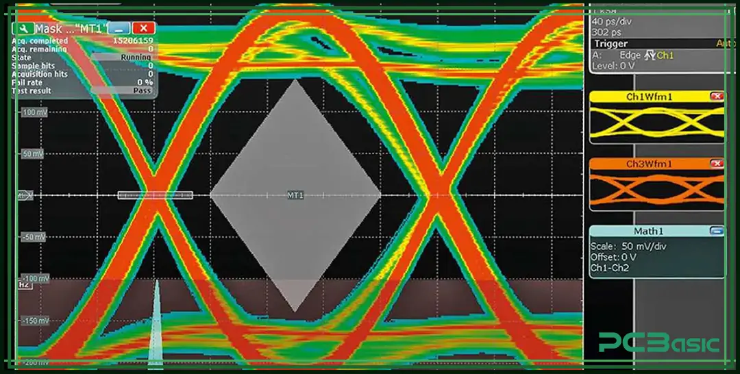
Attenuation compounds from conductor losses, dielectric absorption, and radiation, particularly beyond 10 GHz. Factories employ precise etching tolerances to maintain trace widths, directly impacting resistance. Environmental factors like humidity affect Df, prompting storage protocols in controlled conditions. Testing with vector network analyzers verifies insertion loss post-fabrication. These measures ensure high-frequency PCB quality withstands real-world deployments.
Achieving Precise Impedance Control in PCB Fabrication
Impedance control PCB demands tight tolerances, typically within 10%, to match driver and receiver characteristics. IPC-2141A provides guidelines for calculating microstrip and stripline impedances based on trace width, thickness, and dielectric height. Factories use field solvers during design review and fabricate test coupons for time-domain reflectometry (TDR) verification. Etch factor control during panel processing prevents under-etching that alters geometry. Layer-to-layer registration accuracy ensures reference plane proximity, stabilizing impedance profiles.
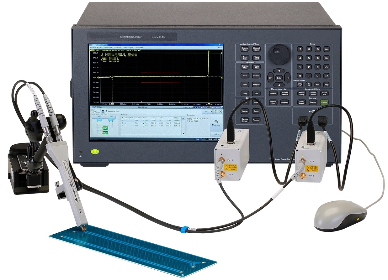
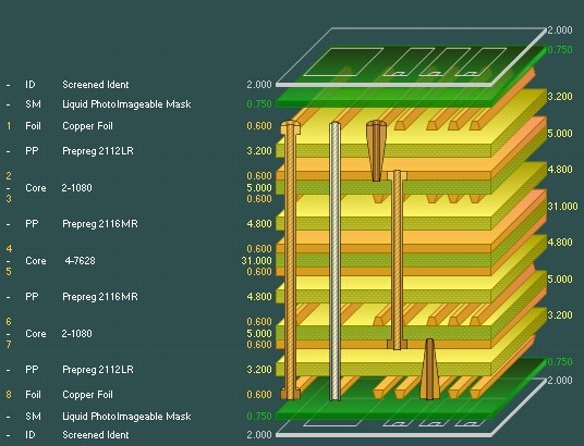
Multilayer boards require sequential build-up with adjusted dielectric thicknesses to hit target values across layers. Plating uniformity affects final trace profiles, addressed through current density optimization in electroplating baths. Post-etch inspection confirms dimensional stability before lamination. Differential pairs for high-speed serial links follow paired trace geometries with controlled spacing. These factory-driven practices deliver reliable impedance control PCB performance.
Manufacturing Best Practices for Superior Quality
Lamination cycles must minimize voids and resin flow inconsistencies, which alter local Dk. Vacuum pressing and controlled ramp rates achieve uniform cure in high-frequency stacks. Drilling parameters adapt to hard substrates, using specialized bits to reduce smear and maintain hole wall integrity. Plasma desmear processes clean residues without damaging dielectrics. Solder mask application requires low-loss formulations to avoid capacitance changes over traces.
Plating baths with additives ensure conformal copper deposition, critical for via reliability. Bake-out procedures remove moisture prior to assembly, preventing popcorning. Final quality checks per IPC-A-600K acceptability criteria inspect for warpage, bow, and twist under thermal cycling. Electrical testing includes flying probe for opens/shorts and dedicated high-frequency fixtures. Traceability from raw material to shipment enables root-cause analysis if issues arise.
Advanced Quality Assurance Techniques
Factory quality control extends to non-destructive testing like automated optical inspection for trace defects. Cross-sectioning samples validates layer alignment and plating thickness. Thermal shock simulations reveal CTE mismatch vulnerabilities. High-frequency specific tests measure S-parameters for return loss and crosstalk isolation. Data logging throughout production supports continuous improvement. These rigorous protocols guarantee high-frequency PCB quality.
Conclusion
High-frequency PCB quality hinges on meticulous material selection, precise impedance control PCB, and robust signal integrity PCB practices. Factory adherence to standards like IPC-6018D and IPC-2141A ensures boards perform reliably in critical applications. Engineers benefit from partnering with manufacturers emphasizing these controls, from design review to final test. Proactive quality measures reduce field failures and accelerate time-to-market. Prioritizing these factors delivers the performance demanded by modern high-speed electronics.
FAQs
Q1: What factors most impact high-frequency PCB quality?
A1: High-frequency PCB quality depends on low-loss materials, uniform dielectric properties, and minimal manufacturing variations. Factories focus on precise trace etching and via control to limit signal losses. Adhering to IPC-6018D standards verifies performance for microwave applications. Proper handling prevents contamination that raises Df. Overall, these elements ensure stable operation above 1 GHz.
Q2: How does impedance control PCB improve signal integrity?
A2: Impedance control PCB maintains consistent characteristic impedance, reducing reflections that distort signals. Guidelines from IPC-2141A aid in trace geometry calculations for microstrips and striplines. Factories verify with TDR on test coupons post-fabrication. This practice minimizes overshoot and preserves timing margins in high-speed designs. Signal integrity PCB thus achieves cleaner waveforms and lower error rates.
Q3: Why is material selection critical for signal integrity PCB?
A3: Material selection affects Dk and Df, directly influencing attenuation and phase stability in signal integrity PCB. Low-loss laminates prevent energy dissipation at high frequencies. Factories test for consistency to avoid hotspots. CTE matching avoids warpage under thermal stress. These choices align with quality standards for reliable high-frequency performance.
Q4: What quality checks ensure high-frequency PCB quality during production?
A4: Production checks include TDR for impedance control PCB, S-parameter testing for losses, and visual inspections per IPC-A-600K. Cross-sections confirm plating and registration. Thermal cycling detects reliability issues. Traceability logs support audits. These steps uphold high-frequency PCB quality from fab to assembly.
References
IPC-6018D — Qualification and Performance Specification for High Frequency (Microwave) Printed Boards. IPC, 2022
IPC-2141A — Design Guide for High-Speed Controlled Impedance Circuitry with Microstrip and Stripline Transmission Lines. IPC, 1996
IPC-A-600K — Acceptability of Printed Boards. IPC, 2020


