Introduction
The rapid proliferation of Internet of Things (IoT) devices has transformed industries, from smart homes to industrial automation. These compact, interconnected systems rely heavily on printed circuit boards (PCBs) to function efficiently. However, the unique design and operational demands of IoT devices introduce specific challenges during PCB rework processes. Rework, which involves repairing or replacing components on a PCB, becomes increasingly complex with the miniaturization and high-density layouts typical in IoT electronics. For electrical engineers, understanding these challenges and mastering rework methods like soldering and component replacement is essential. This article explores the intersection of PCB rework and IoT, delving into technical hurdles and offering practical solutions to ensure reliability and performance in these critical systems.
What Is PCB Rework and Why It Matters in IoT
PCB rework refers to the process of repairing or modifying a printed circuit board by removing, replacing, or adjusting electronic components. This procedure is crucial for correcting manufacturing defects, updating designs, or addressing failures in the field. In the context of IoT, rework takes on heightened importance due to the unique characteristics of these devices. IoT systems often operate in diverse environments, from consumer wearables to industrial sensors, requiring robust and reliable PCBs. A single failure in a connected device can disrupt entire networks, leading to data loss or system downtime. Effective rework methods ensure that defective components are replaced without compromising the board's integrity, maintaining the seamless operation of IoT ecosystems. As IoT adoption grows, mastering rework processes becomes a vital skill for engineers tackling modern electronics challenges.
Technical Challenges of PCB Rework in IoT Devices
IoT devices present several unique obstacles during PCB rework, primarily due to their design and operational constraints. Electrical engineers must navigate these issues to achieve successful outcomes without damaging sensitive components or the board itself.
Miniaturization and High-Density Layouts
IoT devices prioritize compactness, often featuring densely packed components on small PCBs. Surface-mount technology (SMT) components, such as microcontrollers and sensors, are common, with sizes shrinking to 0201 or smaller packages. This miniaturization complicates rework, as soldering and component replacement require precision tools to avoid damaging adjacent parts. The tight spacing also increases the risk of thermal stress during rework, potentially causing pad lifting or trace damage.
Mixed Technology and Material Constraints
Many IoT PCBs incorporate mixed technologies, combining through-hole and SMT components alongside flexible or rigid-flex substrates. These varied materials respond differently to heat during soldering, creating uneven thermal profiles. Excessive heat can warp flexible sections or degrade sensitive materials, while insufficient heat may result in poor solder joints. Engineers must carefully manage thermal exposure to comply with standards like IPC-A-610H, which governs the acceptability of electronic assemblies.
Power and Signal Integrity Concerns
IoT devices often handle low-power signals and high-frequency data transmission, making signal integrity a critical concern during rework. Replacing components can introduce noise or alter impedance if not executed with precision. For instance, re-soldering a radio frequency module without proper alignment can degrade wireless performance. Adhering to guidelines in IPC-6012E for rigid PCB performance ensures that rework does not compromise the board's electrical characteristics.
Environmental and Durability Factors
IoT applications frequently operate in harsh conditions, such as extreme temperatures or high humidity. Rework processes must account for these factors to avoid introducing vulnerabilities. A poorly executed solder joint may fail under thermal cycling, violating reliability standards like JEDEC J-STD-020E for moisture and reflow sensitivity. Engineers need to select appropriate soldering materials and methods to maintain durability post-rework.
Practical Rework Methods for IoT PCBs
Addressing the challenges of PCB rework in IoT devices requires a combination of specialized tools, techniques, and adherence to industry standards. The following methods provide actionable guidance for electrical engineers working on component replacement and soldering tasks.
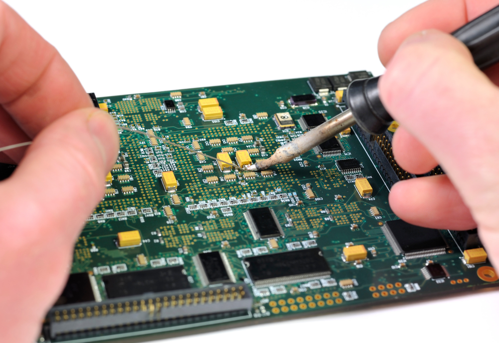
Hot Air Rework for SMT Components
Hot air rework stations are indispensable for handling surface-mount components in these telecom circuit boards. These tools allow controlled heating to remove or replace parts without direct contact, minimizing mechanical stress. Engineers should set temperature profiles based on component specifications and board materials, ensuring compliance with IPC-A-610H for acceptable solder joint formation. Preheating the board reduces thermal shock, especially for multilayer designs common in IoT systems.
Precision Soldering Techniques
Soldering remains a core skill in PCB rework, particularly for fine-pitch components. Using a soldering iron with a fine tip, engineers can manually address small-scale repairs. Temperature control is critical to prevent overheating, which can damage pads or components. Lead-free solder alloys, as recommended by JEDEC J-STD-020E, are often used in IoT devices for environmental compliance, requiring higher melting points and careful handling to form reliable joints.
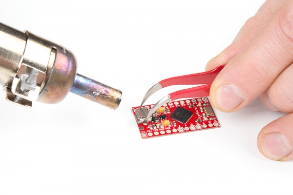
Component Removal and Replacement Best Practices
Removing defective components without damaging the fast turn PCB requires a systematic approach. First, apply flux to reduce surface tension in existing solder joints. Then, use desoldering braid or a vacuum tool to clear excess solder. During replacement, align new components precisely to avoid misalignment, which can disrupt signal integrity. Optical inspection post-rework, as outlined in IPC-A-600K, ensures that no defects remain on the board.
Thermal Management During Rework
Managing heat distribution is essential to prevent warpage or delamination in IoT PCBs. Engineers should use preheaters or heat shields to protect adjacent components during rework. Monitoring thermal profiles with thermocouples helps maintain temperatures within safe limits, aligning with IPC-6012E specifications for board performance. This approach is particularly important for flexible or thin substrates often found in compact IoT designs.
Troubleshooting Common Rework Issues in IoT Electronics
Even with careful planning, rework on IoT PCBs can encounter issues that require troubleshooting. Electrical engineers must identify and resolve these problems to maintain device functionality.
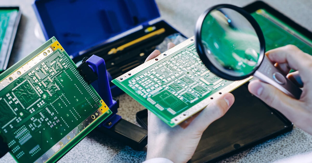
Solder Joint Failures
Poor solder joints, such as cold joints or insufficient wetting, are common after rework. These defects can lead to intermittent connections, disrupting IoT device operation. Visual inspection under magnification, per IPC-A-600K standards, helps detect such issues. Reworking the joint with fresh flux and controlled heat often resolves the problem, ensuring a reliable connection.
Component Damage from Overheating
Excessive heat during soldering can damage sensitive IoT components like microcontrollers or sensors. To mitigate this, engineers should limit exposure time and use heat sinks where possible. Following thermal guidelines in JEDEC J-STD-020E prevents exceeding maximum temperature thresholds during rework processes.
Trace and Pad Repair
Accidental damage to traces or pads during component replacement is a risk in high-density IoT boards. Repair kits with conductive epoxy can restore connectivity, but precision is key to avoid shorts. Adhering to IPC-6012E ensures that repaired areas meet performance criteria for rigid PCBs, maintaining the board's integrity.
Conclusion
PCB rework plays a pivotal role in maintaining the reliability of IoT devices, where compact designs and interconnected systems demand precision and expertise. Electrical engineers face unique challenges, from managing high-density layouts to ensuring signal integrity during component replacement and soldering. By employing specialized rework methods like hot air techniques and adhering to industry standards such as IPC-A-610H and JEDEC J-STD-020E, professionals can address these issues effectively. As IoT continues to shape modern electronics, mastering rework processes remains essential for delivering robust, long-lasting solutions in this dynamic field.
FAQs
Q1: What are the main challenges of PCB rework in IoT devices?
A1: PCB rework in IoT devices is challenging due to miniaturization, high-density layouts, and mixed materials. Compact designs with tiny SMT components require precision soldering to avoid damaging adjacent parts. Thermal management is critical to prevent warpage or signal integrity issues. Engineers must follow strict standards to ensure reliability in diverse operating environments.
Q2: How does soldering impact component replacement in IoT electronics?
A2: Soldering directly affects the success of component replacement in IoT electronics. Proper temperature control prevents overheating sensitive parts, while precise techniques ensure strong joints. Using lead-free solder, as per industry guidelines, meets environmental standards but requires skill to handle higher melting points. Poor soldering can lead to connection failures.
Q3: What rework methods are best for high-density IoT PCBs?
A3: Hot air rework stations are ideal for high-density IoT PCBs, allowing non-contact removal and placement of SMT components. Precision soldering irons suit fine-pitch repairs, while preheating minimizes thermal shock. Following standards like IPC-A-610H during rework processes ensures quality and prevents damage to compact layouts.
Q4: Why is thermal management crucial during PCB rework for IoT?
A4: Thermal management is vital during PCB rework for IoT to avoid damaging components or substrates. Excessive heat can warp boards or degrade materials, especially in flexible designs. Controlled heating, guided by standards like JEDEC J-STD-020E, protects signal integrity and ensures the device remains functional after rework.
References
IPC-A-610H — Acceptability of Electronic Assemblies. IPC, 2021.
IPC-6012E — Qualification and Performance Specification for Rigid Printed Boards. IPC, 2020.
IPC-A-600K — Acceptability of Printed Boards. IPC, 2020.
JEDEC J-STD-020E — Moisture/Reflow Sensitivity Classification for Nonhermetic Surface Mount Devices. JEDEC, 2014.


