Introduction
In the realm of printed circuit board assembly, solderability testing stands as a cornerstone for achieving reliable electrical connections. This process evaluates how effectively molten solder wets and adheres to PCB surfaces, such as pads, lands, and plated-through holes. Poor solderability can lead to joint failures, including incomplete wetting, dewetting, or non-wetting, which compromise product reliability in demanding applications. Electric engineers rely on standardized solderability test methods for PCBs to verify surface finishes and predict assembly performance. By implementing these tests, manufacturers mitigate risks associated with oxidation, contamination, or improper plating. Ultimately, robust solder joints ensure long-term functionality in electronic systems.
What Is PCB Solderability and Why Does It Matter?
Solderability refers to the capacity of a PCB's metallic surfaces to form a strong, uniform bond with molten solder during assembly processes like wave soldering or reflow. It depends on factors such as surface finish quality, cleanliness, and exposure to environmental stressors over time. In high-volume production, inadequate solderability manifests as defects that increase rework costs and yield losses. For electric engineers designing or qualifying PCBs, understanding solderability is essential to select appropriate surface treatments like HASL, ENIG, or OSP. These tests align production with industry expectations for defect-free assemblies. Prioritizing solderability testing directly enhances overall PCB quality control and end-product durability.
Key Solderability Test Methods for PCBs
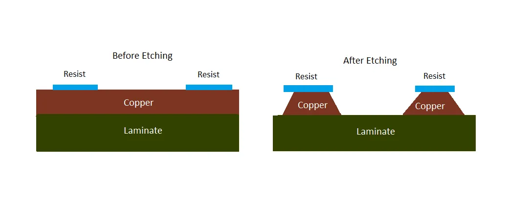
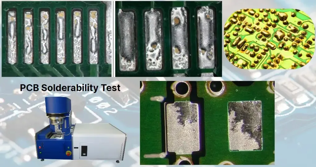
Several solderability test methods for PCBs provide quantitative and qualitative assessments of wetting performance. The solder dip test, also known as dip-and-look, involves fluxing the PCB edge or pads, immersing them in molten solder at specified temperatures, and visually inspecting for coverage. Acceptance criteria typically require uniform solder coating over at least 95 percent of the tested area, with no dewetting or bridging. This method simulates wave soldering conditions and quickly identifies gross defects in surface finishes. Electric engineers appreciate its simplicity for incoming inspections or process validation. Complementary techniques offer deeper insights into wetting dynamics.
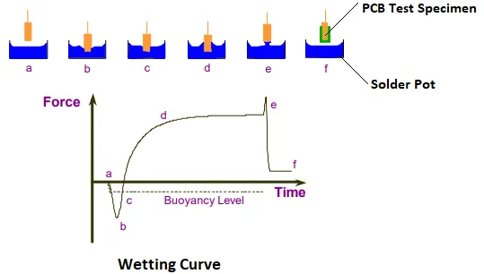
The wetting balance test measures the force exerted by molten solder on a PCB sample as a function of immersion time. In this procedure, a precisely weighed sample dips into fluxed solder, and a load cell records buoyancy and wetting forces, producing a characteristic curve. Good solderability shows rapid meniscus formation and positive force buildup within seconds. This test excels at differentiating subtle differences in finishes, such as immersion tin versus gold, under controlled conditions. Factories integrate it for high-reliability applications where marginal performance could lead to field failures. Data from wetting balance tests guide optimizations in plating thickness and flux selection.
Steam aging serves as a critical preconditioning step in many solderability protocols, simulating long-term storage effects on PCB surfaces. Samples expose to saturated steam environments, accelerating oxidation and intermetallic growth that degrade solderability over time. Post-aging, engineers perform dip or wetting tests to assess retained performance. This reveals vulnerabilities in protective coatings, ensuring PCBs withstand shelf life without re-tinning. In quality control workflows, steam aging test for PCBs confirms compliance before assembly. It proves invaluable for supply chain validation in automotive or aerospace sectors.
Per IPC J-STD-003, these methods define precise procedures, defect classifications, and acceptance thresholds for printed boards. Engineers apply them systematically to correlate test results with assembly yields.
Preconditioning and Environmental Influences on Solderability
Before conducting core solderability tests, preconditioning mimics real-world aging to stress PCB surfaces realistically. Steam aging, for instance, introduces humidity and heat to promote tarnish on exposed copper or tin finishes. This step uncovers latent issues like porosity in plating that flux alone cannot reveal during fresh testing. Electric engineers sequence it with dip-and-look or wetting balance for comprehensive evaluation. Alternative aging, such as baking or reflow simulation, addresses moisture sensitivity in lead-free processes. Proper preconditioning ensures test relevance to actual production timelines and storage conditions.
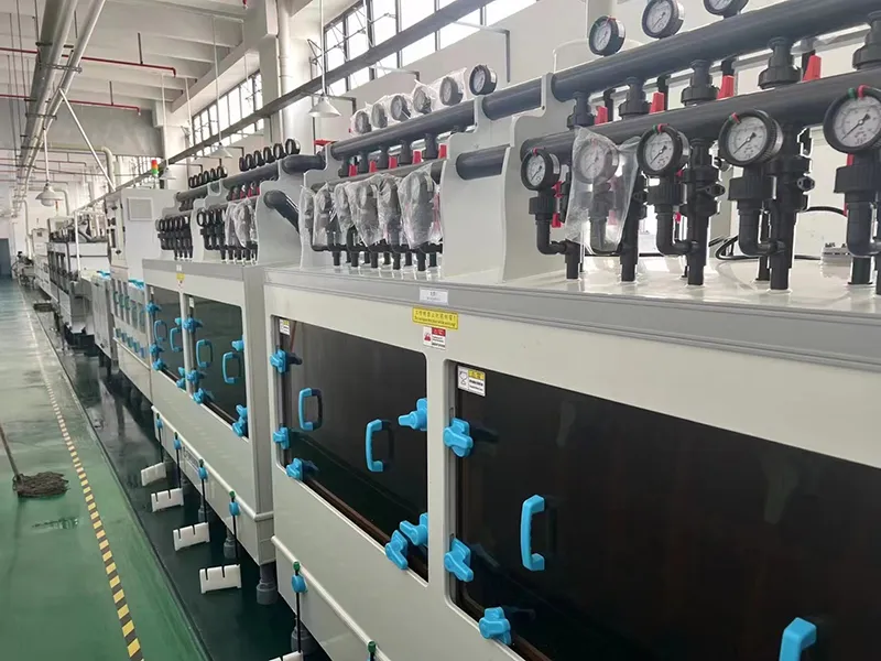
Surface contamination from handling, residues, or halide inclusions further impacts solderability. Factory insights emphasize cleanroom protocols and analytical verification via ion chromatography before testing. Balancing these factors maintains consistency across lots. In turn, this supports scalable manufacturing aligned with quality objectives.
Best Practices for Implementing Solderability Testing
To maximize effectiveness, establish a standardized testing regimen integrated into PCB quality control. Select test methods based on surface finish and assembly type, prioritizing solder dip for high-volume screening and wetting balance for R&D characterization. Calibrate equipment regularly, using certified solder alloys and fluxes to replicate process conditions accurately. Document results with photographs and metrics, correlating them to assembly defect rates for continuous improvement. Train personnel on defect recognition per solderability standards to minimize subjective interpretations.
Collaborate with plating vendors to specify finishes meeting test criteria post-aging. Implement statistical process control on test pass rates, triggering root cause analysis for drifts. For lead-free transitions, adjust immersion times and temperatures to reflect higher melting points. These practices reduce escapes and bolster confidence in PCB reliability. Electric engineers benefit from automating data logging for trend analysis across suppliers.
Incorporate visual aids during evaluations to standardize judgments. Maintain traceability from raw panels to finished boards for failure investigations.
Troubleshooting Common Solderability Failures
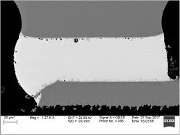
Dewetting, where solder beads up leaving bare metal exposed, often stems from oxidation or contamination unresponsive to flux. Inspect for non-uniform plating or excessive handling prior to testing. Non-wetting indicates severe surface degradation, prompting review of storage practices or finish integrity. Bridging or icicles arise from flux overload or improper withdrawal speeds in dip tests. Use wetting balance curves to pinpoint onset times, guiding flux chemistry tweaks.
Post-steam aging failures highlight inadequate corrosion resistance, necessitating thicker barriers or alternative finishes. Cross-reference with assembly trials to validate fixes. Systematic logging accelerates resolution in factory environments.
Conclusion
PCB solderability testing remains indispensable for guaranteeing robust connections in modern electronics. Methods like the solder dip test, wetting balance test, and steam aging test for PCBs provide actionable data on surface performance. Adhering to solderability standards ensures consistency and reliability across production. Electric engineers armed with these insights optimize designs and processes effectively. Proactive testing minimizes defects, cuts costs, and elevates product quality. Invest in rigorous protocols to future-proof assemblies against evolving challenges.
FAQs
Q1: What are the main solderability test methods for PCBs?
A1: Solderability test methods for PCBs include the solder dip test for visual coverage assessment, wetting balance test for force-time dynamics, and area dip for plated-through holes. Preconditioning via steam aging simulates aging effects. These align with standards like J-STD-003, enabling engineers to qualify surfaces for reliable wetting. Factory implementation focuses on repeatability for quality control.
Q2: How does the wetting balance test evaluate PCB solderability?
A2: The wetting balance test immerses a fluxed PCB sample in molten solder, plotting wetting force against time to quantify meniscus formation speed and strength. Rapid force increase signals excellent solderability, while delays indicate issues like oxidation. It offers precise differentiation over qualitative methods, aiding process optimization in high-reliability builds.
Q3: What role does the steam aging test play in PCB solderability?
A3: Steam aging test for PCBs preconditions samples to accelerate environmental degradation, revealing long-term solderability retention. Performed before dip or wetting tests, it stresses finishes against oxidation. This factory-driven step verifies storage stability, preventing assembly defects from aged stock.
Q4: What are key solderability standards for PCB manufacturing?
A4: Solderability standards like IPC J-STD-003 prescribe test procedures, criteria, and defects for printed boards. They guide wetting balance test, solder dip test, and aging protocols. Engineers reference them for compliance, ensuring uniform industry practices and robust joints.
References
IPC J-STD-003D — Solderability Tests for Printed Boards. IPC, 2023
J-STD-002D — Solderability Tests for Component Leads, Terminations, Lugs, Terminals and Wires. IPC/JEDEC, 2014
IPC-TM-650 2.4.12a — Solderability, Edge Dip Method. IPC