Introduction
PCB via plating forms the backbone of reliable interconnections in printed circuit boards, enabling electrical conductivity across multiple layers. Engineers rely on precise plating techniques to ensure signal integrity and mechanical strength in complex designs. This guide delves into the essentials of PCB plating for vias, covering through-hole plating, blind vias, and buried vias. Understanding these processes helps mitigate failures in high-density interconnects. Factory insights reveal that plating quality directly impacts yield rates and long-term performance. By aligning with established standards, manufacturers achieve consistent results in demanding applications.
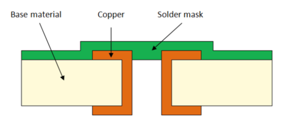
What Are Vias in PCBs?
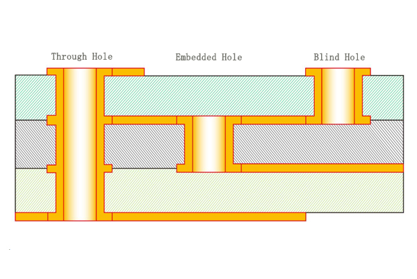
Vias serve as vertical conductors that link different layers in a multilayer PCB. They come in various forms, each suited to specific design needs and manufacturing capabilities. Through-hole vias extend from one surface of the board to the opposite side, providing robust connections for components with leads. Blind vias connect an outer layer to one or more inner layers without penetrating the full board thickness. Buried vias link internal layers exclusively, invisible from the surfaces.
PCB plating transforms these drilled holes into conductive paths by depositing metal, typically copper, on the walls. This process ensures low resistance and adhesion to the substrate. Without proper plating, vias would fail to conduct signals effectively or withstand thermal stresses. Engineers must consider via types early in design to optimize routing density and cost.
Types of Vias and Their Plating Requirements
Through-hole plating involves metallizing holes that traverse the entire board stack-up. These vias support higher current loads due to their larger diameters and full accessibility during plating. Blind vias demand more precise control since plating occurs after partial lamination, limiting electrolyte access. Buried vias, formed between core layers, require sequential plating steps to maintain uniformity.
Each type influences PCB plating strategies differently. For instance, through-hole vias benefit from straightforward panel plating, while blind and buried vias often use pattern plating to focus deposition. Factory processes adjust parameters like current density based on via depth and diameter. Compliance with IPC-6012 ensures plating thickness meets performance specs across these variations. Selecting the right via type balances electrical performance with fabrication feasibility.
The PCB Via Plating Process Step-by-Step
The plating sequence begins with mechanical or laser drilling to create vias in the board material. Desmear removes resin residue from hole walls, exposing a clean surface for adhesion. Electroless copper deposition follows, seeding the walls with a thin conductive layer, typically 0.5 to 1 micrometer thick. This autocatalytic process initiates without external current, ensuring complete coverage even in high-aspect-ratio holes.
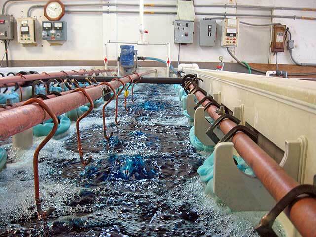
Electroplating then builds up the copper thickness using an acidic bath and direct current. Anodes supply copper ions, while the board acts as cathode, attracting deposition. Agitation and additives control uniformity, throwpower, and grain structure. For blind vias, plating integrates with build-up layers, often requiring multiple electroless-electro cycles. Through-hole plating achieves higher speeds due to open access. Post-plating, inspection verifies coverage via cross-sectioning or electrical testing.
Buried vias plating embeds within cores, plated before lamination. Sequential lamination allows stacking of plated cores for complex boards. Factories monitor bath chemistry to prevent defects like dog-boning, where plating thickens at hole ends. This structured approach aligns with manufacturing realities for reliable outcomes.
Key Technical Principles of Via Plating
Aspect ratio, defined as hole depth divided by diameter, governs plating uniformity. High ratios above 10:1 challenge electrolyte penetration, risking thin spots in hole centers. Copper deposition follows Faraday's laws, where thickness relates to current density and time. Additives like accelerators, suppressors, and levelers fine-tune the process for void-free fills.
Throwpower measures plating efficiency in deep holes, influenced by bath formulation and waveform. Pulse plating enhances coverage over DC for blind vias by improving mass transport. Thermal expansion during plating must match substrate coefficients to avoid cracks. Standards like IPC-A-600 define acceptable plating characteristics, such as minimum thickness and void limits.
Surface preparation ensures strong bonds, with palladium activation aiding electroless initiation. pH, temperature, and impurity control maintain bath stability over production runs. Engineers appreciate these principles for predicting plating outcomes in simulations.
Design Considerations for Optimal Via Plating
Designers specify via sizes considering drill capabilities and plating throwpower. Minimum diameters for through-hole vias typically exceed those of blind vias to accommodate tooling. Annular rings provide landing pads for traces, preventing plating encroachment. Stack-up planning positions buried vias away from edges to minimize stress concentrations.
Fabrication drawings detail plating requirements, including class levels per IPC-6012. Higher classes demand thicker plating and zero voids for mission-critical boards. Signal integrity models account for via stubs in through-hole types, favoring blind or buried for high-speed designs. Cost escalates with via complexity, so trade-offs guide selections.
Best Practices in PCB Plating Manufacturing
Maintain consistent drilling to achieve uniform hole geometry before plating. Automated desmear using plasma or permanganate ensures residue-free walls. Monitor electroless bath for complete seeding via coupon testing. During electroplating, ramp currents gradually to avoid burning at edges.
Factory protocols include frequent hull cell tests for bath analysis. Filtration removes particulates that cause rough plating. Post-plate baking relieves hydrogen embrittlement in copper. For blind and buried vias, align sequential processes tightly to preserve registration. These practices yield high first-pass yields.
Adhering to standards prevents excursions. IPC-6012 outlines qualification for rigid boards, including via plating metrics. Routine audits verify compliance across production lots.
Common Defects in Via Plating and Troubleshooting
Voids appear as gaps in plating, often from trapped air or poor desmear. Cross-section analysis pinpoints locations, tracing back to drilling smear. Cracks result from overplating or thermal mismatch, visible under microscopy. Dogboning thickens ends due to higher current density there, mitigated by suppressor additives.
Black pad or skip plating signals bath contamination, requiring regeneration. For buried vias, misalignment during lamination exposes thin spots. Electrical testing detects opens early. Troubleshooting involves root cause analysis, adjusting parameters like plating time or agitation.
Preventive maintenance on plating lines sustains quality. Training operators on visual cues per IPC-A-600 accelerates issue resolution.
Advanced Techniques for High-Density Vias
Microvia plating supports HDI boards with laser-drilled blind vias under 150 micrometers. Filled vias use conductive epoxy or plated copper for planar surfaces. Via-in-pad designs integrate vias directly under components, demanding precise plating control. These evolve PCB plating beyond traditional through-hole methods.
Sequential build-up layers enable stacked blind vias, multiplying interconnect density. Factories qualify processes for aerospace and telecom demands.
Conclusion
PCB via plating underpins multilayer board reliability, from through-hole plating to sophisticated blind and buried vias. Mastering processes, parameters, and standards ensures robust performance. Engineers benefit from factory-driven best practices to avoid common pitfalls. Prioritizing compliance delivers designs ready for production. This comprehensive approach elevates PCB quality in competitive landscapes.
FAQs
Q1: What is the difference between through-hole plating and blind vias plating?
A1: Through-hole plating coats holes spanning the full board thickness, offering easy access for uniform copper deposition. Blind vias plating targets partial depths from surface to inner layers, requiring sequential processes for electrolyte reach. Both demand electroless seeding first, but blind types face higher aspect ratios. Standards guide thickness uniformity to prevent reliability issues. Factory experience shows blind vias suit high-density routing.
Q2: How does PCB plating affect via reliability in buried vias?
A2: Buried vias plating occurs internally, connecting cores before lamination, emphasizing throwpower for complete coverage. Poor plating leads to high resistance or opens under thermal cycling. Best practices include multiple plating cycles and inspection. IPC guidelines specify acceptance criteria for voids and adhesion. Engineers design with wider margins for these hidden structures.
Q3: What are common parameters controlled in vias PCB plating?
A3: Key controls include current density, bath temperature, and agitation speed to achieve even deposition. Aspect ratio dictates feasible limits for through-hole plating. Additives refine grain size and leveling. Monitoring ensures compliance with plating specs. These factors directly impact signal integrity and mechanical strength.
Q4: Why choose blind vias over through-hole in PCB plating designs?
A4: Blind vias reduce stub inductance for high-speed signals, unlike through-hole vias that penetrate fully. Plating focuses on shorter depths, improving uniformity. They enable denser routing but raise costs due to build-up steps. Suitable for HDI boards per design rules. Balance with buried vias for inner connections.
References
IPC-6012E — Qualification and Performance Specification for Rigid Printed Boards. IPC, 2017
IPC-A-600K — Acceptability of Printed Boards. IPC, 2020
IPC-2221B — Generic Standard on Printed Board Design. IPC, 2012


