Introduction
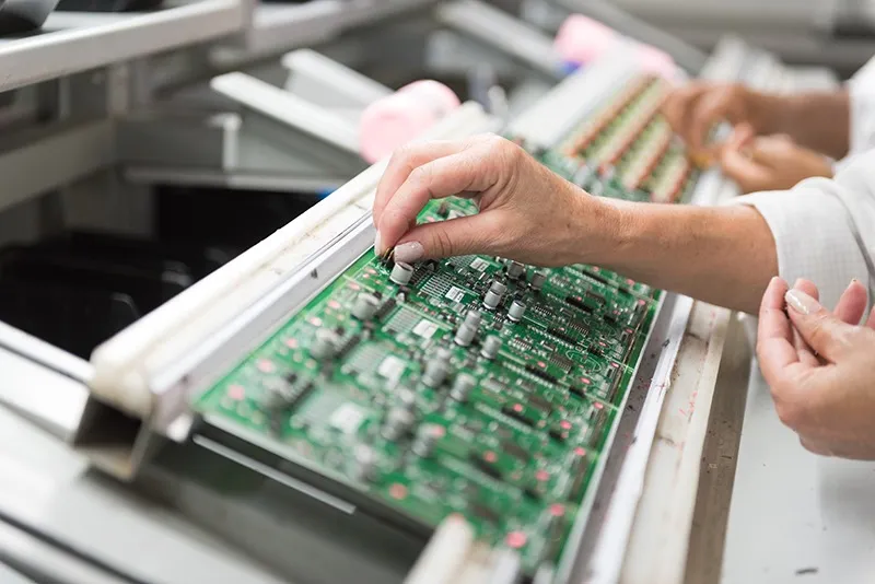
Wave soldering offers hobbyists an efficient way to assemble through-hole components on printed circuit boards, especially when dealing with prototypes or small batches. Unlike hand soldering, which can be time-consuming for multiple joints, this process automates solder application through a flowing wave of molten metal. For electronic hobbyists exploring PCB wave soldering DIY setups, understanding the basics opens doors to professional-grade results at home. This guide breaks down the process step by step, focusing on safety and practicality for beginners. You'll learn how to mimic industrial techniques with accessible tools or a PCB wave soldering kit, ensuring reliable connections without common pitfalls.
What Is PCB Wave Soldering and Why It Matters for Hobbyists
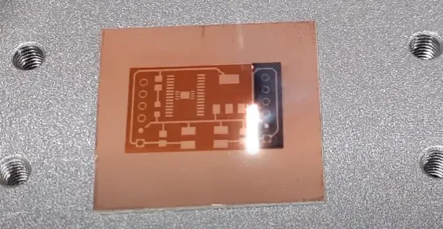
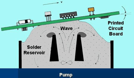
PCB wave soldering involves passing a PCB over a pumped stream of molten solder, which wets the component leads and pads to form strong joints. This method suits through-hole technology, where leads pass through drilled holes and secure on the opposite side. In professional settings, it's ideal for high-volume production, but hobbyists appreciate it for consistency in projects like audio amplifiers or power supplies. Attempting PCB wave soldering at home or with a hobbyist kit speeds up assembly compared to iron soldering, reducing fatigue on larger boards. It matters because proper execution minimizes defects like cold joints, promoting durable electronics that withstand vibration and heat.
The process aligns with industry expectations for through-hole assembly, as outlined in standards like J-STD-001, which specifies requirements for soldered joints. Hobbyists benefit by achieving similar reliability in personal projects, bridging the gap between prototyping and production.
The Technical Principles Behind Wave Soldering
At its core, wave soldering relies on three key stages: flux application, preheating, and solder immersion. Flux cleans oxides from metal surfaces and prevents re-oxidation during heating, ensuring solder flows evenly. Preheating warms the PCB to around 100 to 150 degrees Celsius, reducing thermal shock that could warp boards or crack components. The solder wave, typically tin-lead or lead-free alloy at 250 degrees Celsius, contacts the board underside, filling holes via capillary action.
Different wave types enhance performance; a laminar wave provides smooth flow for fine-pitch leads, while a turbulent wave disrupts the surface to remove oxides better. Cooling follows immediately to solidify joints, preventing movement that causes bridges. These principles ensure fillet formation around leads, a hallmark of quality per IPC-A-610 acceptability criteria.
For hobbyists, grasping these mechanisms helps adapt industrial know-how to simpler setups. Temperature control prevents overheating sensitive parts, while flux choice affects residue cleanup.
Setting Up for PCB Wave Soldering DIY: Equipment and Safety
Start with a well-ventilated workspace, as fumes from flux and solder demand good airflow to protect your health. A basic PCB wave soldering hobbyist setup includes a solder pot with temperature control, capable of melting solder bars into a stable bath. Add a flux applicator, like a spray bottle or brush, and a conveyor-like jig to guide the PCB over the solder surface. Preheat tools, such as an oven or hot plate, maintain board temperature consistency.
Safety gear is non-negotiable: wear gloves, eye protection, and avoid loose clothing near molten metal. Select lead-free solder for modern compliance, aiming for pots holding 1 to 5 kilograms for small projects. Calibrate temperatures with a thermocouple to stay within safe ranges, avoiding splatters or fires.
A PCB wave soldering kit simplifies this, bundling a mini pump for wave generation and controls in a compact unit. Test on scrap boards first to dial in speeds and heights.
Step-by-Step PCB Wave Soldering Tutorial for Beginners
Prepare your PCB by cleaning it and inserting components straight, securing with tape if needed. Apply flux evenly to the underside, focusing on pads and holes to activate surfaces. Preheat the board for 1 to 2 minutes to expand materials uniformly and improve wetting.
Position the PCB parallel to the solder wave at a slight angle, moving it steadily at 1 to 2 meters per minute for home scales. The wave should contact pads briefly, about 3 to 5 seconds, allowing solder to rise through holes. Lift and cool naturally or with forced air to lock joints.
Inspect visually for shiny fillets, full hole fills, and no bridges. Rework any issues with a desoldering tool. This PCB wave soldering tutorial ensures hobbyists achieve repeatable results.
Best Practices for Reliable Through-Hole Assembly at Home
Orient components to avoid shadowing, where tall parts block solder flow to nearby leads. Use pallets or fixtures for double-sided boards to protect surface-mount elements during passage. Maintain solder purity by skimming dross regularly, as impurities degrade joints.
Follow J-STD-001 guidelines for hole fill, targeting at least 75 percent for robust connections. Adjust wave height to match board thickness, preventing excessive solder volume. Clean residues post-process with isopropyl alcohol if using rosin flux.
Panelize multiple small PCBs for efficiency, spacing them to avoid thermal interference. Document your parameters for future batches.
Common Troubleshooting Issues in PCB Wave Soldering Hobbyist Projects
Solder bridges often stem from excessive flux or slow speeds, merging adjacent joints. Reduce speed or tilt the board more to minimize this. Insufficient wetting appears as dull joints; increase preheat or check flux potency.
Icicles form from dripping solder; ensure clean waves and proper cooling. Warpage happens with uneven heating, so use thicker boards or supports. Per IPC-A-610, reject joints with voids larger than 25 percent of pad area.
Test continuity and heat affected components gradually. Patience resolves most issues without scrapping boards.
Advanced Tips for Scaling Your PCB Wave Soldering at Home
Experiment with selective wave techniques using masks for mixed assemblies. Integrate nitrogen atmospheres in enclosed kits to cut oxidation. Monitor with thermal cameras for profile optimization, akin to IPC-9502 process limits.
Batch process similar boards to refine settings. Store flux properly to maintain efficacy.
Conclusion
Mastering PCB wave soldering empowers hobbyists to tackle through-hole projects with speed and precision. From flux prep to final inspection, each step builds reliable assemblies suitable for real-world use. Start simple, prioritize safety, and iterate based on results. Whether using a PCB wave soldering kit or DIY pot, you'll gain skills transferable to larger endeavors. Embrace troubleshooting as learning, and your electronics will reflect professional quality.
FAQs
Q1: What is PCB wave soldering DIY, and is it suitable for beginners?
A1: PCB wave soldering DIY involves using a solder pot or mini machine to flow molten solder over through-hole components on a PCB. It's beginner-friendly with proper safety measures, as it automates joint formation for faster assembly than hand soldering. Follow a PCB wave soldering tutorial to preheat boards and control speeds, achieving consistent results on small projects. Practice on test boards first to build confidence.
Q2: Can hobbyists perform PCB wave soldering at home safely?
A2: Yes, with ventilation, protective gear, and temperature-controlled equipment like a solder pot. PCB wave soldering at home suits low-volume through-hole work, but avoid lead solders if inexperienced. Preheat to prevent cracks, and clean fluxes promptly. Standards like J-STD-001 guide joint quality, helping avoid hazards. Start small to master the process.
Q3: What should I look for in a PCB wave soldering kit for hobbyists?
A3: Seek kits with adjustable temperature, wave pump, and compact size for benches. Features like flux sprayers and preheat zones support reliable through-hole assembly. Ensure compatibility with lead-free solders and easy cleanup. A good PCB wave soldering hobbyist kit simplifies tutorials, reducing defects for projects like Arduino shields. Verify safety certifications.
Q4: How does PCB wave soldering tutorial improve through-hole results?
A4: A PCB wave soldering tutorial teaches fluxing, preheating, and wave contact timing for optimal wetting and fill. It prevents bridges and icicles common in rushed setups. Following steps yields shiny fillets per IPC-A-610, enhancing durability. Hobbyists gain efficiency for multi-board runs.
References
J-STD-001G — Requirements for Soldered Electrical and Electronic Assemblies. IPC, 2017
IPC-A-610H — Acceptability of Electronic Assemblies. IPC, 2019
IPC-9502B — Printed Board Assembly Process Capability Verification. IPC, 2014