Introduction
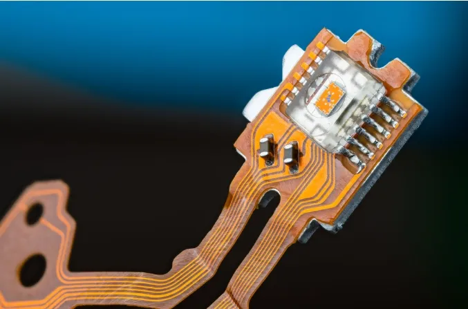
Flexible printed circuit boards (PCBs) have become essential in modern electronics, enabling compact designs in wearables, medical devices, and automotive systems. These flexible circuits rely on thin substrates like polyimide or polyester, which demand precise manufacturing processes to avoid damage. Traditional wet etching methods often introduce chemicals and heat that can cause warpage, delamination, or residue on delicate materials. Plasma etching emerges as a superior alternative, providing gentle etching through low temperature plasma processes. This technique ensures high precision while preserving the integrity of flexible electronics. Engineers working with flexible PCB etching appreciate its ability to meet tight tolerances without compromising substrate flexibility.

Understanding Plasma Etching and Its Relevance to Flexible Circuits
Plasma etching involves generating a plasma from reactive gases to selectively remove material from the PCB surface. In flexible PCB etching, this dry process replaces aggressive wet chemicals, minimizing substrate stress. The plasma consists of ions, electrons, and neutral radicals that chemically and physically etch copper traces or dielectrics. For flexible electronics, where substrates are typically 25 to 125 micrometers thick, plasma etching maintains pattern fidelity without excessive undercutting. Industry standards like IPC-6013 emphasize the need for controlled etching to achieve reliable conductor definition in flexible boards. This method aligns with manufacturing goals for high-yield production of intricate flexible circuits.
Why does plasma etching matter for electric engineers? Delicate substrates in flexible PCBs are prone to thermal expansion mismatches during etching, leading to defects. Plasma processes operate at low temperatures, often below 100 degrees Celsius, classifying them as low temperature etching techniques. This gentleness prevents the warpage seen in conventional methods, ensuring compliance with quality specifications. Engineers benefit from its scalability for high-volume production while supporting fine-line features down to 25 micrometers. Overall, plasma etching enhances the reliability of flexible electronics in demanding applications.
Technical Principles of Plasma Etching
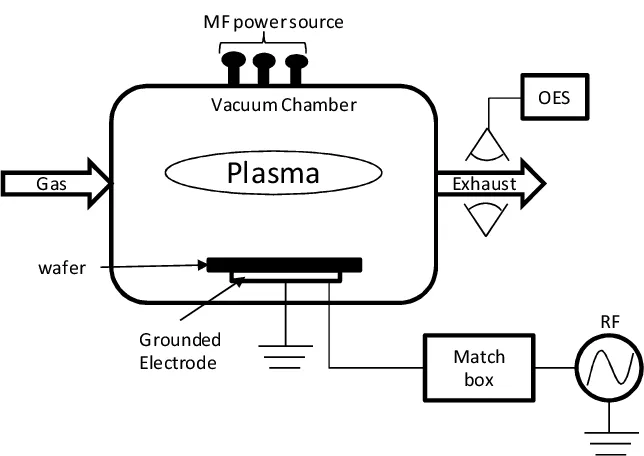
Plasma etching relies on the ionization of gases such as oxygen, fluorine-based compounds, or argon in a vacuum chamber under radiofrequency or microwave energy. The resulting plasma produces reactive species that adsorb onto the substrate surface, facilitating material removal through chemical reactions and ion bombardment. In reactive ion etching (RIE), a directional component enhances anisotropy, ideal for defining sharp sidewalls in flexible PCB traces. For gentle etching, downstream plasma systems separate radicals from ions, reducing physical damage to sensitive polyimide layers. Process parameters like gas flow rate, pressure around 100 to 500 millitorr, and power levels dictate etch rates, typically 50 to 200 nanometers per minute for copper.
Temperature control is critical in plasma etching for flexible circuits. The substrate remains near room temperature due to low plasma density and efficient heat dissipation in vacuum. This low temperature etching avoids softening or degrading the polymer substrate, unlike thermal processes exceeding 150 degrees Celsius. Engineers must select gas chemistries carefully; for example, oxygen plasma excels at organic residue removal, while CHF3 mixtures target copper. Uniformity across large panels is achieved through magnetic enhancement or showerhead gas distribution. These principles ensure reproducible results, supporting the precision required in flexible electronics fabrication.
Advantages of Plasma Etching Over Traditional Methods
Plasma etching offers superior selectivity and minimal residue compared to wet etching, which often leaves undercuts and chemical contamination. In flexible PCB etching, this translates to cleaner sidewalls and better adhesion for subsequent plating or coverlay application. The dry nature eliminates rinse steps, reducing water usage and environmental impact in manufacturing. Engineers note its compatibility with multi-layer flexible circuits, where precise dielectric etching prevents shorts. Low temperature operation preserves mechanical properties, such as bend radius, critical for flexible electronics.
Anisotropy is a key benefit, with etch directionality exceeding 5:1 sidewall angles, enabling denser routing. This contrasts with isotropic wet etching, which broadens traces and compromises signal integrity. Plasma processes also excel in via cleaning and desmear, preparing surfaces per IPC-A-600 acceptability criteria without mechanical abrasion. For delicate substrates, the absence of mechanical stress during gentle etching reduces defect rates. Cost savings arise from higher throughput and fewer rework cycles, making it viable for prototype to production scales.
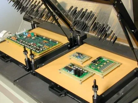
Best Practices for Implementing Plasma Etching in Flexible PCB Manufacturing
Start with surface preparation, including plasma cleaning to remove contaminants before patterning. Optimize etch recipes through design of experiments, varying RF power from 100 to 500 watts and gas ratios for balanced chemistry. Monitor endpoints using optical emission spectroscopy to halt etching precisely, avoiding over-etch into the substrate. Factory-driven insights recommend chamber conditioning between runs to maintain consistency. Regular maintenance of electrodes and pumps ensures stable plasma density.
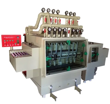
Process control integrates in-line metrology, such as profilometry for etch depth verification. For flexible circuits, handle panels with low-tension fixturing to prevent stretching during transfer. Qualify processes against IPC-6013 requirements for conductor width, spacing, and continuity. Scale-up involves multi-zone plasma tools for uniformity on large sheets. Document all parameters in a controlled quality system, aligning with ISO 9001 principles for traceability.
Challenges and Troubleshooting in Plasma Etching
One common challenge is micro-masking from polymer redeposition, addressed by pulsing the plasma or adding argon for sputtering. Non-uniformity across substrates requires gas distribution optimization and temperature-controlled chucks. Engineers troubleshoot sidewall roughness by adjusting bias voltage, balancing chemical and physical etch components. Substrate charging in thin dielectrics can cause arcing; mitigate with conductive backing or low-frequency power. Yield issues from pinholes stem from inadequate pre-cleaning, resolved by extended oxygen plasma pre-treatment.
For low temperature etching, monitor gas purity to prevent unwanted reactions. Post-etch inspection via cross-sectioning confirms profile integrity. Data logging enables root cause analysis, correlating parameters to defects. These strategies ensure robust processes for flexible electronics.
Conclusion
Plasma etching stands out as a gentle etching solution for flexible PCBs, delivering precision without damaging delicate substrates. Its low temperature operation, anisotropy, and cleanliness make it indispensable for high-performance flexible circuits. Electric engineers gain actionable tools through optimized parameters and standard-aligned practices. By adopting plasma etching, manufacturers achieve superior quality and reliability in flexible electronics. This process future-proofs production amid demands for finer features and miniaturization.
FAQs
Q1: What is plasma etching in the context of flexible PCB etching?
A1: Plasma etching uses ionized gases to remove material precisely from flexible circuits, offering a dry, low temperature alternative to wet methods. It generates reactive species for chemical etching and ion assistance for directionality, ideal for thin copper on polyimide. This gentle etching preserves substrate integrity, enabling fine-line patterns down to 25 micrometers while minimizing warpage.
Q2: Why choose low temperature etching for flexible electronics?
A2: Low temperature etching, like plasma processes, keeps substrates below 100 degrees Celsius, preventing thermal degradation or delamination in flexible PCBs. Traditional methods risk softening polymers, altering flexibility. Engineers prioritize it for maintaining mechanical properties and achieving uniform etch across panels, supporting reliable flexible circuits in compact devices.
Q3: What are the main benefits of plasma etching for flexible circuits?
A3: Plasma etching provides anisotropic profiles, residue-free surfaces, and high selectivity, outperforming wet etching in precision for flexible PCB etching. It reduces defects like undercutting and supports multi-layer builds. Factory processes benefit from scalability and environmental advantages, aligning with quality standards for durable flexible electronics.
Q4: How does plasma etching ensure gentle treatment of delicate substrates?
A4: By isolating radicals in downstream configurations, plasma etching minimizes ion damage while enabling controlled material removal. Low pressure and power settings limit heat, crucial for polyester or polyimide. Pre- and post-process plasma cleaning enhances adhesion without abrasion, ensuring gentle etching throughout flexible PCB manufacturing.
References
IPC-6013E — Qualification and Performance Specification for Flexible and Rigid-Flexible Printed Boards. IPC, 2014
IPC-A-600K — Acceptability of Printed Boards. IPC, 2020
ISO 9001:2015 — Quality Management Systems — Requirements. ISO, 2015