Introduction
In the realm of high frequency electronics, selecting the right printed circuit board material is vital for ensuring optimal performance. Rogers PCB materials have emerged as a preferred choice for high frequency amplifiers due to their excellent dielectric properties and thermal stability. These characteristics are critical for applications such as RF amplifier PCB design and high power amplifier PCB design, where signal integrity and heat dissipation pose significant challenges. This article explores the key attributes of Rogers PCB materials and delves into essential PCB design considerations for high frequency amplifiers. From impedance control to thermal management for amplifier PCBs, the focus is on providing electrical engineers with actionable insights to achieve reliable and efficient designs. Understanding these principles can significantly enhance the performance of advanced electronic systems.
What Is Rogers PCB and Why It Matters
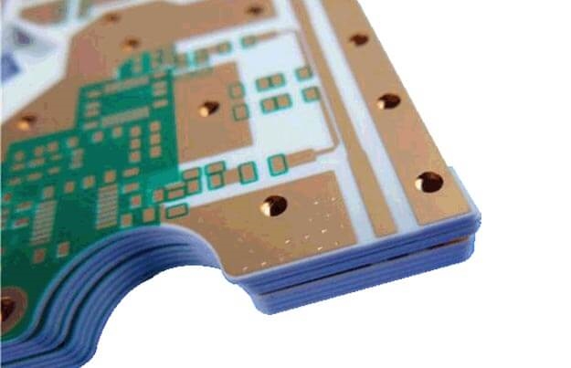
Rogers PCB refers to a family of high performance laminate materials specifically engineered for demanding electrical and thermal environments. Unlike traditional FR-4 materials, these laminates offer low dielectric loss and a stable dielectric constant over a wide range of frequencies. This makes them ideal for high frequency amplifier applications, including RF and microwave circuits. The ability to maintain signal integrity at frequencies above 1 GHz is a key reason why Rogers materials are widely adopted in telecommunications, aerospace, and automotive radar systems.
The significance of using Rogers PCB in high frequency amplifier designs cannot be overstated. In RF amplifier PCB design, minimizing signal loss and ensuring consistent impedance are paramount. Additionally, high power amplifier PCB designs generate substantial heat, requiring materials with superior thermal conductivity. By addressing these challenges, Rogers PCB materials enable engineers to push the boundaries of performance in critical applications.
Technical Principles of Rogers PCB in High Frequency Amplifiers
Dielectric Properties and Signal Integrity
The dielectric constant of a PCB material directly influences the speed and integrity of signals passing through it. Rogers PCB materials are designed with tightly controlled dielectric constants, typically ranging from 2.2 to 10.2, depending on the specific laminate. This control ensures predictable signal propagation, which is crucial for high frequency amplifier circuits operating in the gigahertz range. Low dielectric loss further minimizes energy dissipation, preserving signal strength over long traces.
In RF amplifier PCB design, maintaining signal integrity also involves managing impedance. Mismatched impedance can lead to reflections and signal degradation. Rogers materials support precise impedance control by offering consistent dielectric properties across the board, reducing the risk of performance variations due to material inconsistencies.
Thermal Performance and Stability
High frequency amplifiers, especially in high power applications, generate significant heat during operation. Rogers PCB materials exhibit excellent thermal stability, with glass transition temperatures often exceeding 280 degrees Celsius, ensuring they withstand elevated operating conditions without degrading. This stability is essential for maintaining the mechanical and electrical properties of the board over time.
Moreover, these materials have low coefficients of thermal expansion, which reduces the risk of delamination or cracking under thermal stress. For electrical engineers, this translates to greater reliability in designs where thermal cycling is a concern, such as in aerospace or automotive applications.
PCB Design Considerations for High Frequency Amplifiers
Impedance Matching and Trace Layout
Achieving proper impedance matching is a cornerstone of RF amplifier PCB design. Engineers must design trace widths and spacing to match the characteristic impedance of the system, often 50 ohms in RF applications. Rogers PCB materials facilitate this by providing a stable dielectric constant, allowing for accurate calculations during the design phase. Using simulation tools to model signal paths before fabrication can help identify potential mismatches early.
Trace layout also plays a critical role. Sharp bends in traces can introduce parasitic capacitance and inductance, degrading signal quality. Smooth, gradual curves or mitered corners are recommended to minimize these effects. Additionally, keeping signal traces as short as possible reduces loss and interference in high frequency amplifier circuits.
Ground Plane Design and Noise Reduction
A continuous ground plane is essential for minimizing noise and electromagnetic interference in high frequency designs. Rogers PCB materials support effective grounding due to their low dielectric loss, which helps maintain a clean reference plane for signals. Engineers should ensure that the ground plane is unbroken beneath critical signal paths to avoid discontinuities that could act as antennas for noise.
Via placement is another consideration. Excessive or poorly placed vias can disrupt the ground plane, leading to signal integrity issues. Strategically placing vias to connect ground layers while avoiding signal traces can enhance performance. This approach is particularly important in multilayer boards used for high power amplifier PCB design.
Component Placement and Routing
Component placement significantly impacts the performance of high frequency amplifiers. Critical components, such as transistors and matching networks, should be placed close to each other to minimize parasitic effects. This reduces the length of high frequency signal paths, lowering the risk of loss or interference.
Routing sensitive signals away from noisy power lines or digital circuits is also crucial. Separating analog and digital sections on the board can prevent crosstalk. For multilayer Rogers PCB designs, dedicating specific layers to power and ground planes can further isolate sensitive signals, enhancing overall circuit performance.
Thermal Management for Amplifier PCBs
Heat Dissipation Challenges in High Power Designs
High power amplifier PCB designs often face significant thermal challenges due to the heat generated by active components. Excessive heat can degrade component performance, reduce lifespan, and even cause board failure. Effective thermal management for amplifier PCBs is therefore a critical design consideration.
Rogers PCB materials contribute to thermal management by offering high thermal conductivity compared to standard FR-4. This property allows heat to spread more evenly across the board, reducing localized hot spots. However, material selection alone is not sufficient. Engineers must incorporate additional strategies to ensure adequate heat dissipation.
Strategies for Effective Thermal Management
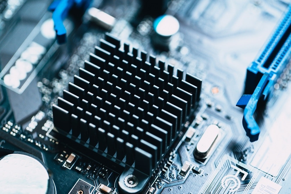
One effective approach is the use of thermal vias. These are small holes filled with conductive material that transfer heat from the top layer to inner layers or a heat sink on the bottom. Placing thermal vias directly beneath heat generating components can significantly improve heat dissipation. Care must be taken to balance the number and size of vias to avoid compromising the structural integrity of the board.
Incorporating heat sinks or metal core layers is another option for high power amplifier designs. These elements provide a direct path for heat to escape from the board. When using Rogers PCB materials, engineers should ensure that the chosen laminate is compatible with metal core integration for optimal thermal performance.
Finally, proper airflow around the PCB can aid in heat removal. Designing enclosures with ventilation or active cooling systems, such as fans, can maintain operating temperatures within safe limits. Combining these techniques with the inherent thermal properties of Rogers PCB materials creates a robust solution for thermal management.
Best Practices for Designing with Rogers PCB
Material Selection Based on Application
Not all Rogers PCB materials are suited for every application. Engineers must select the appropriate laminate based on the frequency range, power requirements, and environmental conditions of the project. For instance, materials with lower dielectric constants are typically chosen for ultra high frequency applications to minimize signal delay, while those with higher thermal conductivity are preferred for high power designs.
Consulting material datasheets for dielectric constant, loss tangent, and thermal properties is a critical step. Matching these parameters to the amplifier’s operational needs ensures optimal performance and reliability.
Suggested Reading: The Ultimate Guide to Choosing the Right Rogers Material for Your PCB
Stackup Design for Multilayer Boards
In multilayer Rogers PCB designs, the stackup configuration influences both electrical and thermal performance. Alternating signal and ground layers can reduce crosstalk and improve signal integrity. Placing power planes adjacent to ground planes can also minimize loop inductance, which is beneficial for high frequency amplifier circuits.
Engineers should work closely with fabrication teams to ensure that the stackup design aligns with manufacturing capabilities. Adhering to guidelines from industry standards, such as those outlined in IPC-6012E, helps maintain consistency and quality during production.
Testing and Validation
Before finalizing a design, thorough testing is essential to validate performance. Signal integrity tests, such as time domain reflectometry, can identify impedance mismatches or signal reflections. Thermal imaging can reveal hot spots or inadequate heat dissipation, allowing for design adjustments.
Following industry standards like IPC-A-600K for acceptability criteria ensures that the fabricated board meets quality expectations. These validation steps are crucial for high frequency amplifier projects where even minor deviations can impact performance.
Conclusion
Designing high frequency amplifiers using Rogers PCB materials offers distinct advantages in terms of signal integrity and thermal stability. By understanding the dielectric and thermal properties of these materials, electrical engineers can make informed decisions to optimize their designs. Key PCB design considerations, such as impedance matching, ground plane integrity, and thermal management for amplifier PCBs, play a pivotal role in achieving reliable performance. Incorporating best practices like strategic component placement, effective heat dissipation techniques, and adherence to industry standards ensures that high power and RF amplifier PCB designs meet the demands of modern applications. With careful planning and validation, Rogers PCB can elevate the efficiency and durability of advanced electronic systems.
FAQs
Q1: What makes Rogers PCB ideal for high frequency amplifier designs?
A1: Rogers PCB materials are ideal for high frequency amplifier designs due to their low dielectric loss and stable dielectric constant. These properties ensure minimal signal loss and consistent impedance, which are critical for maintaining signal integrity in RF amplifier PCB design. Their ability to perform reliably at frequencies above 1 GHz makes them suitable for telecommunications and radar systems.
Q2: How does thermal management for amplifier PCBs impact performance?
A2: Thermal management for amplifier PCBs is crucial as excessive heat can degrade components and reduce lifespan. Effective heat dissipation using thermal vias, heat sinks, and proper airflow prevents performance issues. Rogers PCB materials aid this process with high thermal conductivity, ensuring even heat distribution and protecting high power amplifier PCB designs from thermal stress.
Q3: What are key PCB design considerations for RF amplifier PCB layouts?
A3: Key PCB design considerations for RF amplifier PCB layouts include impedance matching, trace layout, and ground plane design. Engineers must ensure trace widths match system impedance, use smooth bends to avoid parasitic effects, and maintain a continuous ground plane to reduce noise. These steps are essential for preserving signal quality in high frequency circuits.
Q4: Why is material selection important in high power amplifier PCB design?
A4: Material selection in high power amplifier PCB design directly affects thermal and electrical performance. Rogers PCB materials offer high thermal stability and conductivity, mitigating heat related issues. Choosing the right laminate based on power needs and operating environment ensures reliability and efficiency, preventing failures due to thermal or signal integrity problems.
References
IPC-6012E — Qualification and Performance Specification for Rigid Printed Boards. IPC, 2020.
IPC-A-600K — Acceptability of Printed Boards. IPC, 2020.


