Introduction
Selecting the right components for a printed circuit board (PCB) is a critical step in ensuring the functionality, reliability, and efficiency of an electronic system. For electrical engineers, the process involves balancing electrical performance, thermal management, and adherence to industry standards. This article explores the key considerations in choosing PCB components, with a focus on design integration, layout optimization, ground connections, and maintaining appropriate aspect ratios for traces and vias. By understanding these elements, engineers can create robust designs that meet project requirements while minimizing issues like signal interference or thermal stress. The guidance provided here aims to support professionals in navigating the complexities of component selection for optimal PCB performance.
Why Selecting PCB Components Matters
The choice of components directly impacts the overall quality and longevity of a PCB. Components that are mismatched to the design specifications can lead to failures, such as overheating, signal degradation, or mechanical stress. For electrical engineers, selecting components is not just about meeting electrical needs but also about ensuring compatibility with the PCB layout and manufacturing processes. Proper selection reduces the risk of redesigns, cuts down on production delays, and helps maintain compliance with recognized standards. In high stakes applications like aerospace or medical devices, the right components can be the difference between success and catastrophic failure. This process also influences ground connections, which are vital for noise reduction and signal integrity in any circuit design.
Technical Principles of PCB Component Selection
Electrical Compatibility and Performance
When selecting components for a fast turn PCB, engineers must prioritize electrical compatibility with the intended application. This involves matching voltage ratings, current capacities, and power dissipation levels to the circuit requirements. Components like resistors, capacitors, and inductors must be chosen based on their tolerance and frequency response to avoid signal distortion. For active components such as integrated circuits, ensuring pin compatibility and logic levels is essential. Engineers should also consider the impact of parasitic effects, which can alter performance at high frequencies.
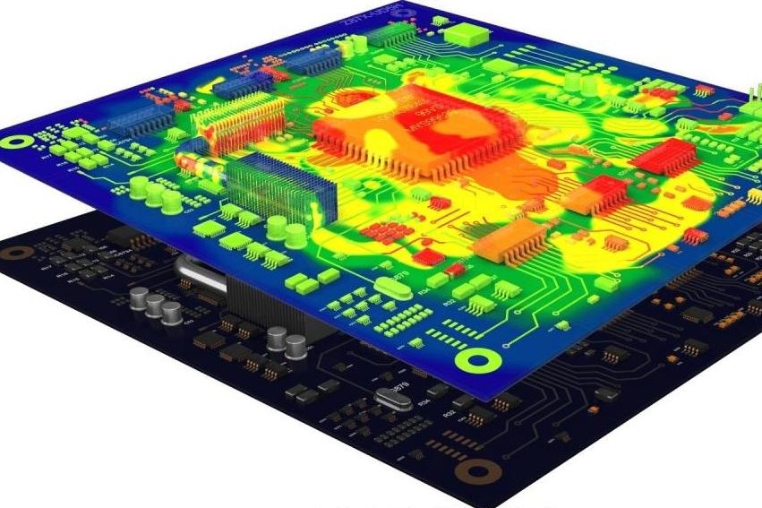
Thermal Management Considerations
Heat dissipation is a significant factor in component selection. Components that generate substantial heat, like power transistors or voltage regulators, require careful placement to avoid thermal hotspots. Selecting components with appropriate thermal ratings and pairing them with heat sinks or thermal vias can mitigate risks. Materials with high thermal conductivity for the PCB substrate also play a role in managing temperature. Standards such as IPC-2152 provide guidelines for current carrying capacity and thermal considerations in PCB design, ensuring components operate within safe limits.
Signal Integrity and Ground Connections
Ground connections are fundamental to maintaining signal integrity and reducing electromagnetic interference (EMI). A well designed grounding scheme, often using a dedicated ground plane, minimizes noise and crosstalk between components. Engineers must select components with low noise characteristics and place them strategically to avoid long return paths. Ground vias should be placed near high speed components to provide a short path to the ground plane. Following guidelines from standards like IPC-2221B helps ensure effective grounding practices in PCB layouts.
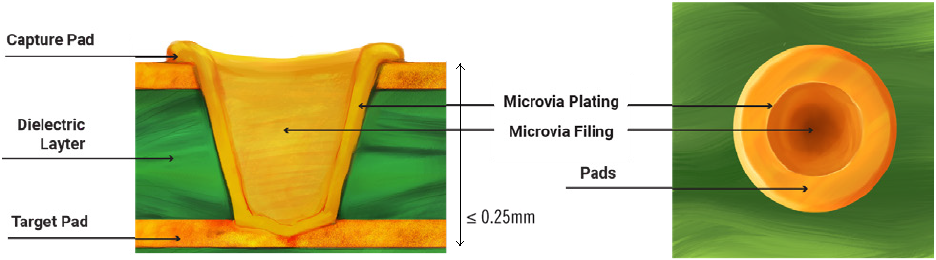
Aspect Ratio in Traces and Vias
The aspect ratio, defined as the ratio of a via's depth to its diameter or a trace's width to its thickness, is crucial for manufacturability and reliability. High aspect ratios in vias can lead to plating issues during fabrication, while improper trace aspect ratios may cause excessive resistance or current density. Engineers must select components and design layouts that allow for balanced aspect ratios, adhering to recommendations in standards such as IPC-6012E. This ensures structural integrity and prevents failures during production or operation.
Best Practices for Selecting PCB Components
Define Design Requirements Early
Before selecting components, engineers should establish clear design requirements. This includes defining operating voltage, current limits, frequency ranges, and environmental conditions. A comprehensive requirements list helps narrow down component choices and prevents costly mismatches. For instance, components for outdoor applications must withstand wide temperature ranges and humidity, as outlined in standards like IPC-A-600K for acceptability criteria.
Prioritize Component Placement in PCB Layout
Component placement in the PCB layout significantly affects performance. Place high speed components close to each other to minimize trace lengths and reduce signal delay. Group components by function, such as analog and digital sections, to avoid interference. Critical components like decoupling capacitors should be near power pins of integrated circuits to stabilize voltage. Adhering to layout guidelines from IPC-2221B ensures optimal placement for signal integrity and thermal balance.
Use Reliable Grounding Techniques
Effective ground connections are non negotiable in PCB design. A continuous ground plane on one layer of a multilayer board provides a low impedance path for return currents. For two layer boards, create ground grids to simulate a plane. Avoid splitting ground planes unless absolutely necessary for isolating noisy sections. Place ground vias strategically near components with high switching speeds to reduce loop areas, following best practices in IPC-2221B.
Select Components with Standard Footprints
Choosing components with standardized footprints simplifies PCB design and manufacturing. Footprints that align with industry standards reduce the risk of errors during assembly and ensure compatibility with automated placement equipment. Engineers should refer to libraries based on IPC-7351B for land pattern design to maintain consistency. This practice also aids in sourcing components from multiple suppliers without redesigning the layout.
Verify Aspect Ratio Compliance
When selecting components and planning the PCB layout, ensure that trace widths and via dimensions comply with acceptable aspect ratios. For vias, a depth to diameter ratio below 10:1 is generally recommended by standards like IPC-6012E to avoid fabrication challenges. For traces, maintain a width to thickness ratio that supports the expected current without overheating, as guided by IPC-2152. These ratios contribute to a manufacturable and reliable design.
Consider Lifecycle and Availability
Component availability over the product lifecycle is a practical concern. Selecting components with long term availability or multiple sourcing options prevents delays in production due to obsolescence. Engineers should also consider lead times and regional availability when choosing parts. While specific supplier data cannot be referenced, adhering to widely accepted component standards like JEDEC J-STD-020E for moisture sensitivity ensures compatibility with assembly processes.
Troubleshooting Common Issues in Component Selection
Addressing Signal Integrity Problems
Signal integrity issues often arise from poor component selection or placement. High speed components with mismatched impedance can cause reflections and data errors. Engineers can mitigate this by selecting components with specified impedance characteristics and using controlled impedance traces in the PCB layout. Ground connections must be robust, with vias connecting to the ground plane near signal transitions. Standards like IPC-2221B offer detailed guidance on maintaining signal integrity through design.
Managing Thermal Overloads
Thermal overloads occur when components exceed their temperature ratings due to poor selection or inadequate heat dissipation. To troubleshoot, review the power ratings of components and ensure they match the circuit demands. Adding thermal vias or increasing copper thickness near heat generating parts can help. Following thermal design guidelines from IPC-2152 ensures that the PCB layout supports effective heat management without compromising component reliability.
Resolving Manufacturing Defects
Manufacturing defects can stem from selecting components with non standard footprints or high aspect ratio requirements that strain fabrication limits. If defects occur, review the component datasheets against design rules specified in IPC-6012E. Adjust the layout to accommodate more manufacturable aspect ratios for vias and traces. Consulting acceptability criteria in IPC-A-600K can also guide engineers in identifying and correcting issues related to component integration.
Suggested Reading: Troubleshooting Guide: Common PCB Component Failures and Their Root Causes
Conclusion
Selecting PCB components is a multifaceted process that requires careful consideration of electrical, thermal, and mechanical factors. By focusing on compatibility, optimizing the PCB layout, ensuring robust ground connections, and maintaining appropriate aspect ratios, electrical engineers can design reliable and efficient circuits. Adherence to industry standards provides a framework for making informed decisions, reducing the risk of failures during production or operation. Through systematic selection and strategic design practices, engineers can achieve high performance PCBs that meet the demands of modern electronic applications.
FAQs
Q1: How does PCB design impact component selection?
A1: PCB design significantly influences component selection by defining electrical and spatial constraints. Engineers must choose components that fit the layout, match voltage and current needs, and support signal integrity. Standards like IPC-2221B guide placement and routing to ensure compatibility. Proper selection aligned with design prevents issues like noise or thermal stress, ensuring the board performs as intended in its application.
Q2: What role do ground connections play in PCB performance?
A2: Ground connections are vital for reducing noise and maintaining signal integrity in a PCB. A solid ground plane minimizes EMI and crosstalk by providing a low impedance return path. Placing ground vias near high speed components shortens current loops. Following IPC-2221B ensures effective grounding, which is crucial for stable operation, especially in mixed signal or high frequency designs.
Q3: Why is aspect ratio important in PCB layout?
A3: Aspect ratio in vias and traces affects manufacturability and reliability in a PCB layout. High via depth to diameter ratios can cause plating defects, while improper trace ratios may lead to resistance issues. Standards like IPC-6012E recommend balanced ratios to avoid fabrication challenges. Maintaining proper aspect ratios ensures structural integrity and consistent performance across the board.
Q4: How can engineers optimize PCB layout for component placement?
A4: Optimizing PCB layout involves grouping components by function and minimizing trace lengths for high speed signals. Place decoupling capacitors near power pins to stabilize voltage. Use standards like IPC-7351B for consistent footprints to ease assembly. Strategic placement reduces interference and thermal hotspots, enhancing overall board reliability and performance in demanding applications.
References
IPC-2221B — Generic Standard on Printed Board Design. IPC, 2012.
IPC-6012E — Qualification and Performance Specification for Rigid Printed Boards. IPC, 2020.
IPC-A-600K — Acceptability of Printed Boards. IPC, 2020.
IPC-7351B — Generic Requirements for Surface Mount Design and Land Pattern Standard. IPC, 2010.
IPC-2152 — Standard for Determining Current Carrying Capacity in Printed Board Design. IPC, 2009.
JEDEC J-STD-020E — Moisture/Reflow Sensitivity Classification for Nonhermetic Surface Mount Devices. JEDEC, 2014.


