Introduction
Selective gold plating represents a targeted approach in PCB manufacturing where gold is applied only to specific areas requiring enhanced conductivity, corrosion resistance, and durability. This method contrasts with full board plating techniques by minimizing material usage and focusing on critical features like contacts and edge connectors. Engineers often specify selective gold plating for applications demanding high reliability under frequent mating cycles or harsh environments. The process aligns with industry needs for cost efficiency without compromising performance. As gold prices fluctuate, understanding selective gold plating vs full board plating becomes essential for optimizing designs in electric engineering projects. This guide explores the technical aspects, cost factors, and best practices to aid informed decision-making.
What Is Selective Gold Plating and Why It Matters
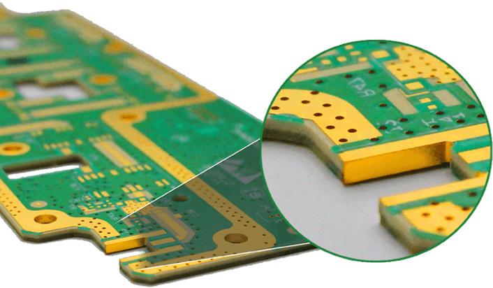
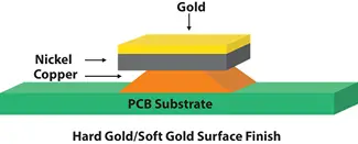
Selective gold plating involves electrolytic deposition of hard gold onto designated copper or nickel surfaces on a PCB, while other areas remain protected by masking materials. This technique ensures thick, wear-resistant gold layers precisely where needed, such as on connector pads or high-wear zones, without covering the entire board. Full board alternatives like electroless nickel immersion gold provide uniform thin gold but lack the hardness for intensive contact applications. Selective plating matters because it balances superior electrical performance with economic viability, particularly in high-volume production. For electric engineers, it supports compliance with performance specifications in IPC-6012 for rigid printed boards. Ultimately, this method extends PCB lifespan in demanding sectors like aerospace and telecommunications.
Selective Gold Plating vs Full Board Plating
Selective gold plating targets specific features, reducing gold consumption compared to full board plating, which coats the entire surface uniformly. In selective gold plating vs full board plating scenarios, the former uses electrolytic hard gold for superior abrasion resistance, ideal for repeated insertions, while full board often employs softer immersion gold for solderability across pads. Full board plating simplifies processing but increases material costs and risks signal integrity issues from unnecessary coverage. Selective approaches demand precise masking but yield lower overall expenses, especially as plated area shrinks. Engineers must evaluate mating cycle requirements and environmental exposure to choose appropriately. Cost savings from selective methods can significantly impact project budgets without sacrificing reliability.
- Coverage: Specific areas (e.g., contacts)
- Gold Type: Hard (electrolytic)
- Primary Use: High-wear connectors
- Cost Driver: Masking and setup
- Thickness Control: Precise on targets
Technical Principles of Selective Gold Plating
The process begins after pattern plating and solder mask application, where a temporary mask covers non-plating areas to expose only the target copper traces or pads. Electrolytic gold plating then deposits a hard alloy of gold and cobalt or nickel, achieving high purity and hardness through controlled current density. Adhesion relies on an underlying nickel strike layer to prevent diffusion and ensure long-term stability. Post-plating, the mask strips cleanly, revealing protected surfaces ready for assembly. This sequence adheres to standards like IPC-4552 for electroless nickel immersion gold preparation in hybrid finishes. Variations include partial immersion for edge plating, optimizing uniformity on bevels.
Cost Analysis of Selective Gold Plating
The cost of selective gold plating hinges on several interconnected factors, starting with the surface area requiring plating, as gold constitutes the dominant expense due to its market value. Smaller plated zones, such as edge fingers covering under 5% of the board, drastically cut material use compared to full coverage. Masking techniques add labor and material costs, but economies scale with volume, where setup amortization benefits high-mix production. Process complexity, including rack fixturing for electrolytic baths and waste treatment, influences per-unit pricing. Selective gold plating vs full board plating often shows 30-50% savings in prototypes, widening in production runs. Engineers should model costs based on design footprint, gold spot price, and fab capabilities to justify specifications.
Additional variables include plating thickness demands, driven by wear cycles, and post-process inspections for voids or porosity. Nickel underlayer thickness affects total cost, as thicker barriers enhance reliability but raise expenses. Yield rates improve with refined masking, reducing rework. Procurement teams benefit from quoting multiple area configurations to benchmark the cost of selective gold plating. Ultimately, lifecycle savings from durability offset initial premiums in high-reliability applications.
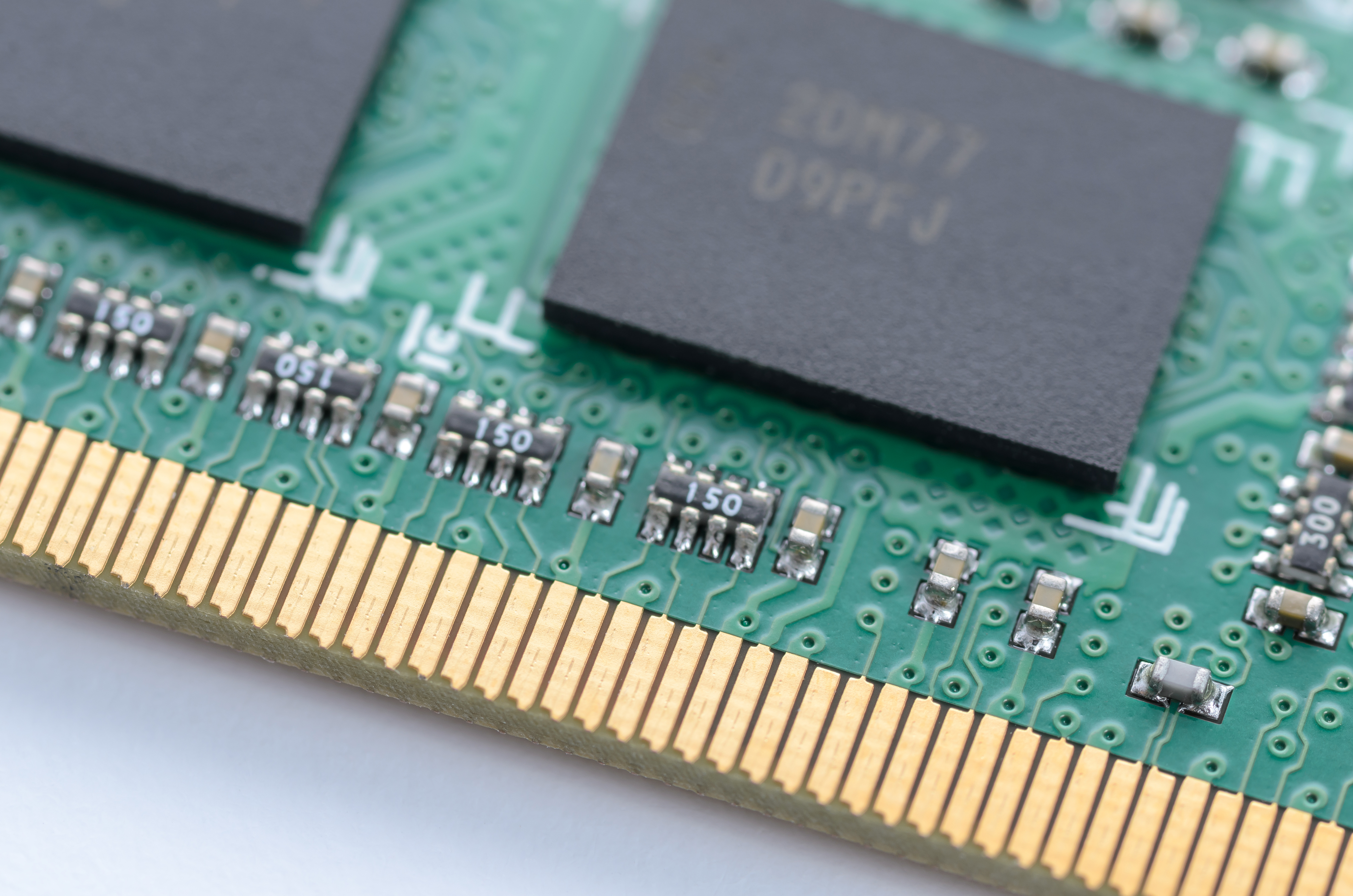
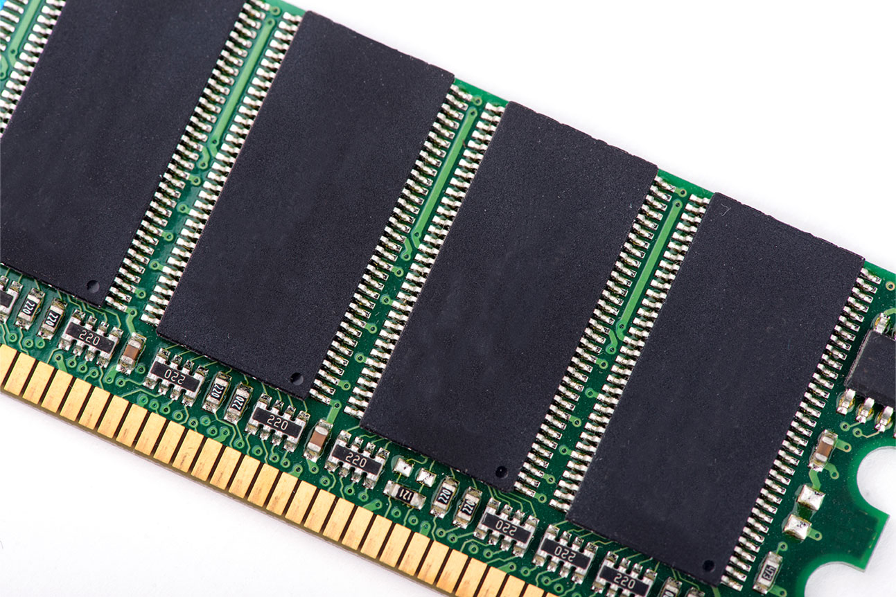
Applications: Selective Plating for Connectors and High-Wear Areas
Selective plating for connectors excels in edge card designs, where gold fingers endure thousands of insertion cycles without fretting corrosion. Hard gold on bevelled edges ensures low contact resistance and stable signals in backplane systems. High-wear areas, like battery contacts or test probes, leverage selective plating to withstand mechanical stress and oxidation. In automotive electronics, these zones resist vibration-induced failures. Aerospace modules use selective plating for RF connectors demanding low insertion loss. Factory insights confirm selective plating for high-wear areas extends mean time between failures in mission-critical hardware.
Masking Techniques for Selective Plating
Masking techniques for selective plating primarily employ dry film photoresist, laminated over the board and exposed via artwork aligned to plating targets. Liquid photoimageable soldermasks offer finer resolution for complex patterns, developing to expose precise features before plating. Peelable masks, cured temporarily, suit irregular geometries and strip without residue post-plating. Each method requires compatibility with plating chemistries to avoid contamination or undercutting. Dry film suits high-volume edge plating, while liquid excels in pad arrays. Proper tenting prevents bleed, ensuring sharp boundaries per IPC-A-600 acceptability criteria.
Application involves clean surface preparation, uniform coating, and bake cycles for adhesion. Exposure controls line widths down to production tolerances. Development rinses reveal plating windows cleanly. Engineers select based on feature density and throughput needs. Validation through cross-sections verifies mask integrity.
Best Practices for Implementing Selective Gold Plating
Design panels with plating areas grouped for efficient racking, minimizing handling damage and bath contamination. Specify nickel underplate thickness adequate for diffusion barriers, balancing cost and performance. Collaborate with fabricators early to align masking resolution with line widths. Implement automated optical inspection post-strip to detect plating anomalies like dog-boning. Control plating parameters, including current ramp-up, to achieve uniform deposits. For selective plating for connectors, bevel edges at 30 degrees to optimize contact wipe.
Test prototypes under accelerated wear per application cycles to validate thickness retention. Maintain bath chemistry through regular analysis for consistent hardness. Document fab notes clearly, noting standards compliance. Scale from prototypes by panelizing designs efficiently. These practices ensure reliable outcomes across production.
Conclusion
Selective gold plating offers electric engineers a precise, cost-effective solution for enhancing PCB reliability in critical interfaces. By contrasting selective gold plating vs full board plating, designers prioritize wear resistance where essential, slashing unnecessary expenses. Key applications in connectors and high-wear areas underscore its value in demanding environments. Masking techniques and best practices further refine implementation for optimal results. Overall, informed cost analysis guides specifications toward balanced performance and economy. Adopting these insights streamlines engineering workflows and elevates product durability.
FAQs
Q1: What are the main advantages of selective gold plating vs full board plating?
A1: Selective gold plating vs full board plating reduces gold usage significantly by targeting only high-wear areas, lowering the cost of selective gold plating while providing thicker, harder deposits for better durability. Full board methods suit broad solderability but inflate expenses. Engineers gain precise control over performance zones, aligning with IPC standards for efficiency. This approach suits connectors needing frequent mating.
Q2: How does the cost of selective gold plating vary with design factors?
A2: The cost of selective gold plating depends on plated area, masking complexity, and production volume, with smaller zones yielding substantial savings over full coverage. High gold prices amplify benefits for edge connectors. Volume production amortizes setup costs effectively. Engineers optimize by minimizing footprint without performance trade-offs.
Q3: What masking techniques for selective plating are most reliable for connectors?
A3: Masking techniques for selective plating include dry film for edge fingers and photoimageable for pads, ensuring clean exposure in selective plating for connectors. These prevent bleed and support fine pitches. Peelable options aid irregular shapes. Selection hinges on resolution needs for high-wear reliability.
Q4: When should selective plating for high-wear areas be specified?
A4: Selective plating for high-wear areas fits applications like test points or battery contacts enduring abrasion and corrosion. It outperforms thinner finishes in extended cycles. Specify for backplanes or automotive modules per performance specs. Cost benefits emerge in targeted use.
References
IPC-6012E — Qualification and Performance Specification for Rigid Printed Boards. IPC, 2015
IPC-4552B — Specification for Electroless Nickel/Immersion Gold (ENIG) Plating for Printed Circuit Boards. IPC, 2012
IPC-A-600K — Acceptability of Printed Boards. IPC, 2020