Introduction
In the realm of high-frequency electronics, RF and microwave PCBs demand exceptional signal integrity and minimal losses to support applications like telecommunications, radar systems, and satellite communications. Sequential lamination emerges as a critical fabrication technique in RF PCB lamination, enabling the construction of complex multilayer structures with precise control over layer thickness and via interconnections. Unlike conventional single-cycle lamination, this process involves multiple bonding cycles, allowing engineers to incorporate blind, buried, and stacked vias essential for high-density designs. For microwave PCB fabrication, sequential lamination for RF applications addresses the unique challenges of signal propagation at frequencies exceeding 1 GHz, where dielectric properties and impedance stability become paramount. By optimizing the buildup of layers, it minimizes crosstalk and insertion loss, ensuring reliable performance in demanding environments. This article explores the principles, practices, and benefits of sequential lamination, providing factory-driven insights for electric engineers designing next-generation high-frequency boards.
What Is Sequential Lamination and Why It Matters for RF and Microwave PCBs
Sequential lamination refers to a multilayer PCB fabrication method where sub-stacks or subsets of copper foils, cores, and prepregs are bonded in successive cycles, typically two or more, to form the final board. Each cycle includes imaging, drilling, plating, and lamination, enabling advanced via structures like microvias that connect specific layers without penetrating the entire stack. In high-frequency PCB materials contexts, this approach surpasses traditional lamination by allowing hybrid constructions that integrate low-loss dielectrics tailored for RF signals. For electric engineers, its relevance lies in supporting higher layer counts and denser routing, crucial for microwave PCB fabrication where space constraints and performance demands converge. Without sequential lamination, achieving the necessary via density and layer precision in RF designs becomes impractical, leading to compromised signal paths. Ultimately, it aligns with industry needs for boards that maintain electrical stability across wide frequency bands.
The process matters profoundly in high-frequency applications because standard laminates often fail to deliver the controlled impedance in RF PCBs required for minimal reflections and maximum power transfer. Sequential builds facilitate exact dielectric thickness control between signal and ground planes, vital at microwave frequencies where even minor variations cause phase shifts or attenuation. Factory experience shows that this technique reduces manufacturing variability, enhancing yield for complex RF assemblies. Moreover, it supports the integration of specialized high-frequency PCB materials with differing thermal expansions, preventing defects during assembly.
Technical Principles of Sequential Lamination in High-Frequency Applications
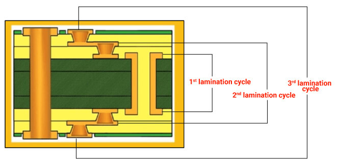
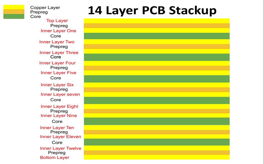
The core principle of sequential lamination begins with preparing a central core or sub-composite, typically 2 to 4 layers, followed by sequential addition of outer layers using thin dielectric films and copper foils. After initial lamination and patterning, laser drilling creates precise microvias for the next cycle, which are then plated before bonding additional layers. This iterative process, often limited to 2-3 cycles for optimal results, builds asymmetric or symmetric stackups suited to RF PCB lamination needs. In microwave PCB fabrication, the technique excels by isolating sensitive signal layers, reducing parasitic capacitance and inductance that degrade high-frequency performance. Engineers must account for via stub minimization, as stacked microvias shorten signal paths compared to through-holes.
Dielectric flow during each lamination cycle fills gaps uniformly under controlled pressure and temperature, ensuring void-free bonds critical for signal integrity. High-frequency PCB materials with low dielectric constant and dissipation factor are selected to maintain consistent propagation velocity. The sequential nature allows registration accuracy better than mechanical limits, preserving trace geometries for controlled impedance in RF PCBs. As per IPC-6018 guidelines for high-frequency boards, this method verifies performance through electrical testing post each cycle.
Selecting High-Frequency PCB Materials for Sequential Lamination
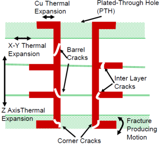
High-frequency PCB materials form the foundation of successful sequential lamination for RF, characterized by stable dielectric constants, low loss tangents, and matched coefficients of thermal expansion. These materials, often resin systems reinforced with low-expansion glass, resist deformation during multiple heat-pressure cycles inherent to the process. In RF PCB lamination, low Z-axis CTE prevents via barrel cracking or delamination when bonding disparate layers. Factory insights emphasize materials with high glass transition temperatures to withstand repeated thermal excursions without resin degradation.
Compatibility between core and buildup films is paramount; mismatched properties lead to stress concentrations around vias. Sequential lamination benefits from thin, resin-rich prepregs that flow adequately to encapsulate traces and vias, promoting uniform thickness for impedance stability. For microwave PCB fabrication, materials enabling low surface roughness on copper further reduce skin effect losses at elevated frequencies. Adherence to IPC-4103 specifications ensures these laminates meet high-speed performance criteria.
Best Practices for Sequential Lamination in Microwave PCB Fabrication
Limit lamination cycles to 2-3 to balance complexity with reliability, as additional cycles amplify stress accumulation and registration errors. Begin with a robust central core featuring plated through-holes, then apply symmetric buildup on both sides to minimize warpage in high-frequency PCB materials. Precise alignment using pins during layup maintains layer-to-layer registry, essential for via capture in dense RF designs. Post-lamination, implement planarization to ensure flatness before subsequent imaging.
Material pairing demands low-modulus buildup dielectrics over high-Tg cores to absorb expansion differentials. Retain sufficient surface copper on sub-stacks for balanced thermal stress distribution during bonding. In controlled impedance in RF PCBs, model stackups iteratively to predict dielectric spacing needs before fabrication. Cleanliness protocols between cycles prevent contamination that could introduce voids or adhesion failures.
Achieving Controlled Impedance in RF PCBs Through Sequential Lamination
Controlled impedance in RF PCBs hinges on precise dielectric thickness and material uniformity, both enhanced by sequential lamination's layer-by-layer control. Engineers specify trace widths, spacings, and heights per simulation, then verify post-fabrication with time-domain reflectometry. The process allows embedding ground planes adjacent to signal layers, tightening coupling for 50-ohm or 100-ohm differentials common in microwave applications. Hybrid stackups integrate high-frequency sections seamlessly, avoiding transitions that disrupt impedance profiles.
Via optimization via laser drilling reduces discontinuities, preserving return loss margins. Factory-driven practice involves multiple test coupons on panels to correlate modeled and measured values. Sequential builds facilitate finer adjustments, such as varying prepreg ply counts per layer for gradient impedances.
Challenges and Mitigation in Sequential Lamination for RF
Primary challenges stem from coefficient of thermal expansion mismatches, where resin expands far more than copper or glass during lamination, risking cracks or delamination. Warpage in asymmetric stackups exacerbates via stress, particularly in thicker boards. Moisture absorption prior to cycles can induce popcorn effects, compromising bonds.
Mitigation includes symmetric designs, low-CTE materials, and controlled ramp rates in presses. Pre-bake panels to remove volatiles, and use filled vias to equalize expansion. J-STD guidelines aid in process qualification, ensuring robustness for high-frequency service.
Conclusion
Sequential lamination stands as a cornerstone for RF PCB lamination and microwave PCB fabrication, delivering the precision and density required for high-frequency performance. By enabling advanced via structures and material hybridization, it optimizes controlled impedance in RF PCBs while upholding signal integrity. Electric engineers benefit from its flexibility in addressing thermal and electrical challenges through informed stackup design and process controls. Adopting best practices minimizes risks, yielding reliable boards compliant with industry benchmarks. As demands for higher frequencies intensify, sequential lamination remains indispensable for cutting-edge applications.
FAQs
Q1: What role does sequential lamination play in RF PCB lamination for high-frequency signals?
A1: Sequential lamination builds multilayer RF PCBs through multiple bonding cycles, allowing precise microvia placement and layer isolation. This enhances signal integrity by minimizing stubs and enabling tight impedance control. Factory processes limit cycles to 2-3, using low-CTE high-frequency PCB materials to prevent defects. Overall, it supports denser routing essential for GHz-range performance without compromising reliability.
Q2: How does sequential lamination for RF improve controlled impedance in RF PCBs?
A2: It provides exact control over dielectric thicknesses between signal and reference planes via iterative buildup. Laser-drilled vias reduce discontinuities, while uniform prepreg flow ensures consistent propagation constants. Engineers model stackups to achieve 50-ohm lines, verified post-lamination. This factory-aligned method outperforms single-cycle lamination for microwave frequencies.
Q3: What are key high-frequency PCB materials considerations in microwave PCB fabrication using sequential lamination?
A3: Select materials with low dissipation factors, stable Dk, and matched Z-axis CTE to endure multiple cycles. High-Tg resins resist thermal stress, while resin-rich films promote void-free bonds. Compatibility prevents delamination, aligning with standards for RF performance. These choices optimize loss and stability in sequential builds.
Q4: Why limit lamination cycles in sequential lamination for RF applications?
A4: Excessive cycles increase CTE mismatch risks, leading to warpage or via failures in high-frequency designs. Two to three cycles suffice for most HDI RF needs, balancing density with yield. This practice maintains registration and impedance uniformity during microwave PCB fabrication.
References
IPC-6018D — Qualification and Performance Specification for High Frequency (Microwave) Printed Boards. IPC
IPC-4103B — Specification for Base Materials for High Speed/High Frequency Applications. IPC
IPC-6012E — Qualification and Performance Specification for Rigid Printed Boards. IPC


