Introduction
Silkscreen, also known as the legend layer, plays a critical role in printed circuit board design by providing essential visual cues for assembly, testing, and maintenance. In multi-layer PCBs, where component density and complexity increase significantly, effective silkscreen design becomes even more vital to ensure reliability and ease of use. Engineers must consider factors like layer stackup, manufacturing processes, and post-assembly visibility to avoid common pitfalls. This article explores best practices for silkscreen in multi-layer boards, focusing on placement strategies, visibility challenges, and overlap prevention. By adhering to these guidelines, designers can enhance board performance and reduce production errors. Proper silkscreen implementation supports seamless integration in high-density electronics.
What Is Silkscreen and Why It Matters in Multi-Layer PCBs
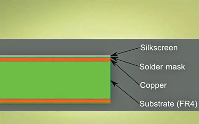
Silkscreen refers to the non-conductive ink printed on the PCB surface, typically over the solder mask, to denote component identifiers, polarity marks, test points, and regulatory symbols. In single-layer or double-sided boards, silkscreen application is straightforward, but multi-layer PCBs introduce unique challenges due to buried traces and components. These boards often feature six or more layers, with inner layers dedicated to power planes, ground, and signals, making outer surface real estate precious. Effective silkscreen ensures technicians can quickly locate and verify components during assembly or rework, minimizing errors in complex designs. Without clear markings, troubleshooting multi-layer boards becomes time-consuming and error-prone, potentially leading to field failures. Industry standards like IPC-A-600 emphasize legibility and durability of these markings to meet quality benchmarks.
The relevance grows in applications like telecommunications and automotive electronics, where multi-layer boards handle high-speed signals and dense routing. Poor silkscreen can obscure critical information, complicating inspection after reflow soldering or conformal coating. Designers must balance information density with manufacturability, ensuring silkscreen aids rather than hinders the process. In essence, silkscreen bridges design intent with practical fabrication and use.
Technical Principles of Silkscreen in Multi-Layer PCB Fabrication
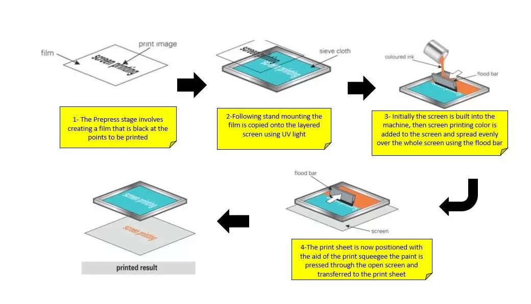
Silkscreen ink is applied after lamination and solder mask imaging, exclusively on the top and bottom outer layers of multi-layer PCBs. Inner layers, encapsulated within prepreg and core materials during high-pressure lamination, cannot accommodate silkscreen due to inaccessibility and process incompatibility. Instead, inner layers may feature etched copper identifiers for fabrication alignment, but these are not visible post-manufacture. The silkscreen process involves screen printing, liquid photoimaging, or direct legend printing, cured via UV exposure for adhesion and solvent resistance. This sequence ensures the legend withstands assembly stresses like wave soldering or infrared reflow without smearing or lifting.
Visibility in multi-layer boards hinges on contrast between ink and solder mask, typically white ink on green mask for optimal readability. Layer stackup influences silkscreen indirectly, as asymmetric builds or thin dielectrics can cause warpage, potentially cracking surface inks. Engineers must account for via types, blind and buried vias reduce outer clutter but demand precise marking of accessible features. Adherence to IPC-2221 guidelines for clearances prevents defects from ink migration during thermal cycling.
Silkscreen Placement on Inner Layers: Myths and Realities
Silkscreen placement on inner layers is not feasible in standard multi-layer PCB manufacturing, as these layers undergo etching and lamination before outer finishes. Attempts to apply ink internally would be encapsulated and invisible, offering no practical benefit for assembly or debug. Some designers confuse etched copper artwork on inner planes with silkscreen, using it for fab notes like layer numbers or date codes. These etchings aid stackup verification during production but disappear in the final board. For visibility, critical inner layer information must migrate to outer silkscreen, duplicating identifiers for buried passives or fiducials.
In complex designs, prioritizing outer placement prevents misalignment during panelization or routing. IPC-6012 specifies qualification for surface features, reinforcing that inner markings remain production-only aids. Engineers should use design rules to flag invalid inner silkscreen attempts early.
Ensuring Silkscreen Visibility in Multi-Layer Boards
Silkscreen visibility in multi-layer boards depends on strategic placement adjacent to components, avoiding obstruction by tall parts or enclosures. Post-assembly, capacitors and resistors may shadow markings, so position reference designators offset but proximate for quick reference. Contrast remains key, with ink selection matching solder mask color to maintain legibility under LED shop lights or magnification. In dense multi-layer layouts, group related labels to form readable zones, reducing visual clutter.
Manufacturing tolerances affect visibility, as misalignment between silkscreen and copper can blur edges. Test visibility by simulating fab outputs at 1:1 scale, checking from multiple angles. For high-reliability boards, matte inks reduce glare compared to glossy finishes.
Avoiding Silkscreen Overlap in Complex PCBs
Avoiding silkscreen overlap in complex PCBs requires disciplined clearance rules from pads, vias, and traces to prevent ink intrusion during soldering. Overlaps compromise solderability, create shorts, or obscure fiducials needed for pick-and-place accuracy. In multi-layer designs, high via density exacerbates risks, so maintain uniform spacing around blind vias emerging on surfaces. Design automation helps enforce minimum gaps, flagging violations before Gerber export.
Prioritize essential markings like pin-1 dots and polarity bars, relocating non-critical text to board edges or secondary layers. Layer stackup planning influences overlap potential, as inner signal routing dictates outer via fields. Regular design reviews catch overlaps early, ensuring compliance with fabrication limits.
- Pads and SMD footprints — Enforce 5-mil minimum annular clearance.
- Through-hole vias — Offset labels radially around via perimeter.
- Test points — Reserve halo zones free of ink.
- Fiducials — Dedicate 1mm x 1mm clear areas.
Best Practices for Silkscreen Design in Multi-Layer PCBs
Start with component libraries incorporating standardized silkscreen overlays, ensuring pin-1 and outline accuracy. Limit text rotation to 0 or 90 degrees for readability, aligning with board outline flow. Use sans-serif fonts scaled appropriately for density, favoring simplicity over decoration. In multi-layer, document buried nets via outer legends, enhancing debug without X-ray reliance.
Color selection impacts visibility, white suiting most masks while black aids light backgrounds. Validate designs against fab DFM checks, iterating for overlap-free layouts. Consistent naming conventions streamline assembly across variants.
Troubleshooting Common Silkscreen Issues in Multi-Layer Designs
Blurry legends often stem from thin stroke widths or poor ink adhesion, resolvable by thickening lines and selecting qualified polymers per IPC-SM-840. Misregistration appears in high-layer-count boards from stackup shifts, countered by fiducial arrays tying silkscreen to copper. Fading post-reflow indicates solvent incompatibility, addressed via bake-out cycles pre-printing.
In complex PCBs, overlaps surface during panelization, fixed by v-groove aware placement. Field reports of invisible inner labels highlight duplication needs, prompting outer redundancies.
Conclusion
Mastering silkscreen design for multi-layer PCBs demands attention to outer-layer exclusivity, visibility optimization, and rigorous overlap avoidance. By duplicating key inner info externally and enforcing clearances, engineers mitigate risks in dense layouts. Standards like IPC-A-600 guide acceptability, ensuring durable, legible boards. Implementing these practices streamlines manufacturing, assembly, and long-term reliability. Future designs benefit from automated checks, evolving with higher layer counts.
FAQs
Q1: Can silkscreen be placed on inner layers of multi-layer PCBs?
A1: No, silkscreen placement on inner layers is not possible in standard processes, as these layers are laminated internally and inaccessible for ink application. Visibility requires duplicating essential markings on outer top and bottom layers. This approach maintains assembly efficiency without compromising board integrity. Consult stackup diagrams for inner etch aids used in fabrication only.
Q2: How do you ensure silkscreen visibility in multi-layer boards during assembly?
A2: Silkscreen visibility in multi-layer boards relies on high-contrast inks, strategic proximity to components, and avoidance of shadowing by tall parts. Position labels offset from SMD bodies and use simple fonts for post-reflow clarity. Grouping related designators forms scannable zones. Validate under production lighting to confirm legibility.
Q3: What are key strategies for avoiding silkscreen overlap in complex PCBs?
A3: Avoiding silkscreen overlap in complex PCBs involves setting design rule clearances around pads, vias, and traces, typically minimum gaps enforced in EDA tools. Prioritize critical labels and relocate others to edges. Mirror bottom silkscreen in Gerbers for alignment. This prevents soldering defects and fiducial obstruction.
Q4: Why duplicate silkscreen for inner components in multi-layer designs?
A4: Duplicating silkscreen for inner components ensures identification when buried elements are inaccessible, aiding troubleshooting without dissection. Outer layers carry reference designators and values, compensating for multi-layer opacity. This practice reduces errors in high-density boards. It aligns with standard assembly workflows.
References
IPC-A-600K — Acceptability of Printed Boards. IPC, 2020
IPC-2221B — Generic Standard on Printed Board Design. IPC, 2012
IPC-6012E — Qualification and Performance Specification for Rigid Printed Boards. IPC, 2017
IPC-SM-840D — Qualification and Performance of Permanent Solder Mask. IPC, 2004


