Introduction
In compact PCB designs, every square millimeter counts toward achieving functionality, reliability, and manufacturability. Silkscreen, the printed legend layer that includes reference designators, polarity marks, and assembly instructions, often competes for precious surface real estate. Poor placement can lead to illegible markings, assembly errors, or even manufacturing rejects. Engineers face the challenge of balancing information density with readability in high-density interconnect boards. This article explores compact PCB silkscreen tips to help optimize space without compromising quality. By applying structured strategies, designers can minimize silkscreen footprint effectively.
What Is Silkscreen and Why It Matters in Compact Designs
Silkscreen refers to the non-conductive ink layer applied to the PCB surface, typically in white or contrasting colors, to convey critical information like component identifiers and orientation cues. This layer aids technicians during assembly, inspection, and rework by providing visual references that survive soldering processes. In compact designs, where component pitch shrinks to 0.3 mm or less, silkscreen becomes vital yet constrained by limited available space. Overcrowded or poorly placed silkscreen can obscure pads, interfere with fiducials, or violate clearance rules, increasing defect rates. Prioritizing silkscreen placement ensures compliance with assembly workflows and reduces troubleshooting time in production environments. Ultimately, effective silkscreen management supports faster prototyping and higher yields in space-limited applications.
The relevance intensifies in sectors like consumer electronics and IoT devices, where board sizes dwindle to credit-card dimensions. Without thoughtful silkscreen strategies, engineers risk misaligned components or prolonged debug sessions post-assembly. Standards like IPC-A-600 define acceptability criteria for legend legibility, emphasizing its role in quality control. In tight spaces, silkscreen must convey maximum utility with minimal intrusion.
Technical Principles of Silkscreen in PCB Fabrication
Silkscreen application follows a photo-imaging process similar to solder mask, where UV-sensitive ink cures under masked exposure to form precise patterns. Line widths and character heights must exceed fabrication tolerances to prevent bleeding or incomplete curing, especially on fine-pitch boards. Minimum stroke widths typically range from 4 to 6 mils to ensure durability through reflow soldering and cleaning steps. Character heights should allow readability from 12 inches away under standard lighting, guiding minimum dimensions for production stability.
Material properties influence placement decisions, as silkscreen ink adheres best to bare laminate or solder mask surfaces but avoids exposed copper to prevent shorts. Thermal expansion during assembly can distort fine features if placed near high-stress areas like vias or edges. IPC-6012 outlines performance specifications for rigid boards, including legend registration to maintain alignment across layers. Understanding these mechanisms allows engineers to predict how silkscreen interacts with board warpage or flexure in compact layouts.
Registration accuracy depends on panelization and exposure equipment, demanding offsets from board edges to accommodate tolerances. In multilayer compact designs, top and bottom silkscreen layers require coordination to avoid conflicting information. These principles form the foundation for placing silkscreen in tight spaces, ensuring the final product meets functional and aesthetic requirements.
Challenges of Silkscreen in High-Density Environments
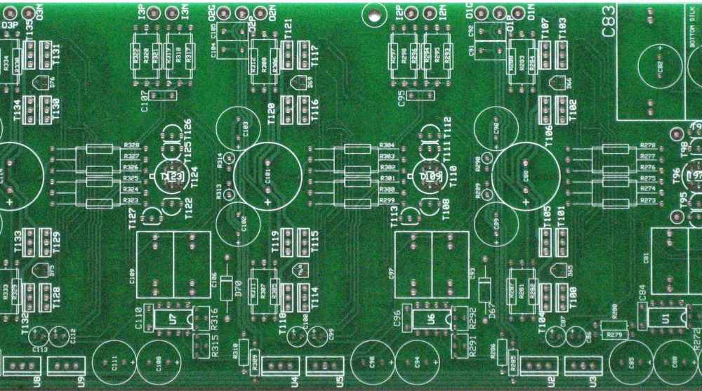
Compact PCBs amplify challenges like pad overlap, where silkscreen encroaches on solder joints, risking contamination or inspection failures. Fine-pitch BGA or QFN components leave scant room for reference designators, forcing trade-offs between completeness and space. Edge proximity introduces smearing risks during depaneling, while fiducial marks demand clear zones free of ink. Overlapping silkscreen with test points hinders probing, complicating functional verification.
Density also affects readability under magnification, as clustered labels blend without adequate spacing. Component shadows post-assembly obscure underlying silkscreen, underscoring the need for elevated or peripheral placement. These issues compound in HDI boards with microvias, where layer stacking limits surface access. Addressing them requires foresight during schematic capture and layout phases.
Compact PCB Silkscreen Tips: Minimizing Footprint Effectively
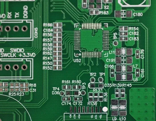
Start by prioritizing essential markings: include only reference designators, polarity indicators, and pin-1 notches for critical parts, omitting verbose descriptions. Abbreviate labels where possible, such as using "R" for resistors or "TP" for test points, to shrink text blocks without losing meaning. Rotate text to align with board flow, maximizing horizontal space utilization in linear arrays. These compact PCB silkscreen tips reduce overall footprint by up to 30 percent in constrained areas.
Position silkscreen outside component courtyards, adhering to IPC-7351 guidelines for footprint outlines that keep legends clear of solder fillets. Maintain minimum clearances of 5 mils from pads and 10 mils from edges to prevent ink migration during printing. Group related labels into zones, such as along board borders or between signal groups, to create breathing room centrally. Vertical stacking with consistent baselines improves density while preserving scanability.
Leverage both silkscreen layers judiciously: place top-side info for surface-mount parts and bottom-side for through-hole, avoiding redundancy. Use geometric symbols like arrows or bars for orientation instead of words, conserving space in ultra-compact zones. Simulate post-assembly visibility in design tools to validate placements early. These strategies exemplify minimizing silkscreen footprint systematically.
Best Practices for Placing Silkscreen in Tight Spaces
Adopt a minimum font height of 25 mils with 5 mil stroke width as a baseline for legibility in production lighting, scaling down only for non-critical info. Ensure uniform line thickness to avoid weak points prone to cracking under thermal cycling. Orient all text horizontally or at 90 degrees for intuitive reading, following left-to-right and bottom-to-top conventions. Consistent polarity markings, such as beveled corners for diodes, standardize identification across the board.
Incorporate keep-out zones around fiducials and optical marks, typically 0.1 inch diameter clear circles. For BGA areas, route silkscreen along grid lines between balls rather than over them. Validate designs against fabrication DFM reports to catch violations pre-production. Bullet-point checklists streamline reviews:
- Prioritize component designators over logos.
- Avoid silkscreen over vias or mounting holes.
- Test contrast against solder mask color.
- Confirm no overlap with assembly adhesives.
These practices ensure placing silkscreen in tight spaces enhances rather than hinders manufacturability.
Troubleshooting Common Silkscreen Issues in Compact Designs
Illegible smudges often stem from insufficient clearance or thin strokes; increase margins iteratively during layout. Assembly feedback reveals hidden labels, prompting relocation to exposed peripheries. Manufacturing rejects for registration errors highlight the need for fiducial alignment checks. Simulate ink bleed by inflating silkscreen polygons in design verification.
When space exhausts, migrate info to documentation or QR codes etched subtly, though legibility trumps novelty. Cross-reference with IPC-A-600 acceptability classes to classify defects preemptively. Iterative prototyping refines placements, balancing density with usability.
Conclusion
Optimizing silkscreen placement transforms compact PCB challenges into reliable designs ready for high-volume production. By embracing compact PCB silkscreen tips like prioritization, strategic positioning, and standard clearances, engineers minimize silkscreen footprint without sacrificing essential information. Adhering to principles from IPC-6012 and related guidelines ensures legibility and durability. These approaches not only streamline assembly but also elevate overall board quality. Implement them systematically to unlock efficiency in your next tight-space project.
FAQs
Q1: What are the key compact PCB silkscreen tips for high-density boards?
A1: Focus on essential markings only, use abbreviations, and position labels outside component courtyards with 5-mil pad clearances. Minimum 25-mil character heights maintain readability. Orient text logically and simulate post-assembly visibility. These steps minimize footprint while aiding technicians.
Q2: How can engineers minimize silkscreen footprint without losing functionality?
A2: Prioritize reference designators and polarity symbols, grouping them in border zones. Employ geometric indicators over text where possible. Adhere to IPC-7351 for footprint silkscreen rules. Validate with DFM analysis to avoid overlaps. This preserves space for routing in compact layouts.
Q3: What clearances are recommended when placing silkscreen in tight spaces?
A3: Maintain at least 5 mils from solder pads, 10 mils from edges, and clear zones around fiducials. Avoid vias and test points to prevent interference. Consistent stroke widths of 5 mils ensure print quality. These rules support reliable manufacturing per industry norms.
Q4: Why does silkscreen placement matter in compact PCB designs?
A4: It prevents assembly errors, aids inspection, and complies with standards like IPC-A-600 for legend acceptability. Poor placement risks smearing or obscuration, inflating costs. Optimized strategies enhance yields and debug speed in space-constrained applications.
References
IPC-A-600K — Acceptability of Printed Boards. IPC, 2020
IPC-6012E — Qualification and Performance Specification for Rigid Printed Boards. IPC, 2017
IPC-7351D — Generic Requirements for Surface Mount Design and Land Pattern Standard. IPC, 2010


