Introduction
In PCB assembly, solder joints serve as the fundamental connections between components and the board, directly influencing the overall reliability and performance of electronic devices. Poor solder joint quality can lead to intermittent failures, reduced lifespan, and costly rework, making it a persistent challenge in surface-mount technology processes. Engineers often encounter issues during reflow soldering, where thermal dynamics and material interactions dictate joint formation. Understanding solder defects PCB and implementing robust solder joint inspection methods becomes essential for maintaining high yields. This article explores the mechanisms behind these vulnerabilities, common pitfalls, and proven strategies for reflow soldering quality control. By focusing on practical troubleshooting, it equips electric engineers with actionable insights to strengthen assembly outcomes.
Why Solder Joint Quality Matters in PCB Assembly
Solder joints must withstand mechanical stresses, thermal cycling, and electrical loads throughout a product's lifecycle. A compromised joint compromises signal integrity, power delivery, and structural integrity, potentially causing field failures in applications from consumer electronics to automotive systems. In high-volume production, even a small defect rate amplifies costs through scrap, rework, and warranty claims. Industry benchmarks emphasize that reliable joints correlate with adherence to established criteria, such as those in IPC-A-610 for acceptability. For electric engineers, prioritizing solder joint quality ensures compliance with performance specs and accelerates time-to-market. Ultimately, it forms the backbone of dependable PCB assemblies.
Common Solder Defects in PCB Assembly
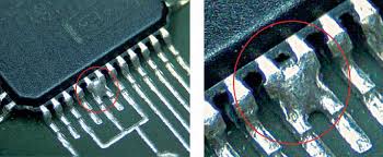
Solder defects PCB manifest in various forms, each with distinct visual and functional signatures. Solder bridges occur when excess solder connects adjacent pads, creating unintended shorts that disrupt circuit operation. Tombstoning, or the Manhattan effect, happens when one end of a chip component lifts due to uneven reflow, leading to open circuits. Cold joints appear dull and grainy, indicating incomplete melting and poor wetting, which compromises mechanical strength. Voids and blow holes within the joint trap gases, reducing cross-sectional area and risking fatigue failure under vibration. Insufficient wetting leaves pads partially exposed, weakening adhesion between solder and surfaces. Recognizing these solder defects PCB early through systematic solder joint inspection prevents downstream issues.
Root Causes of Solder Defects During Reflow Soldering
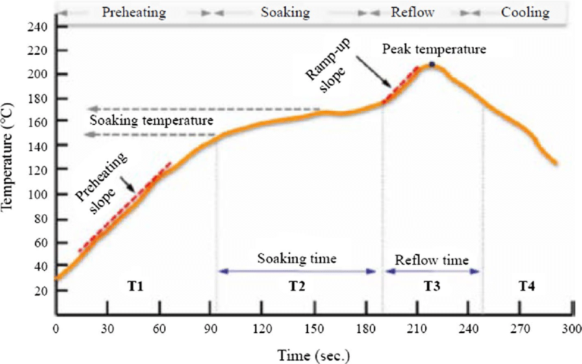
Reflow soldering quality control hinges on managing thermal profiles, where preheat, soak, reflow, and cool-down phases dictate alloy behavior. Improper preheat can cause solder paste to splatter, leading to insufficient solder volume and open joints. Excessive peak temperatures promote rapid flux burnout, generating voids as outgassing overwhelms the joint. Component misalignment stems from board warpage or stencil printing inaccuracies, exacerbating tombstoning in fine-pitch devices. Poor flux activity fails to remove oxides, resulting in cold joints with inadequate intermetallic formation. Environmental factors like humidity introduce moisture sensitivity, aligning with classifications in IPC/JEDEC J-STD-020. Engineers must trace these causes back to process parameters for targeted corrections.
Solder Joint Inspection Techniques for Electric Engineers
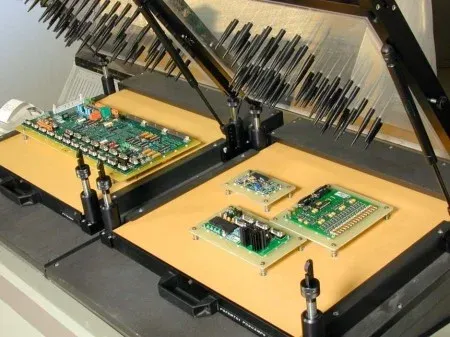
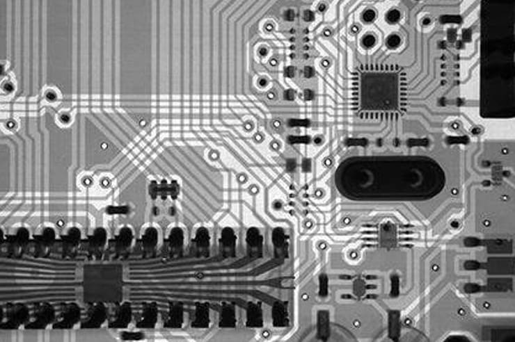
Effective solder joint inspection combines visual, automated, and advanced methods to detect defects at multiple stages. Manual visual inspection identifies obvious issues like bridges or misalignment using magnification and lighting, serving as a first-line defense. Automated optical inspection scans for shape anomalies, fillet dimensions, and wetting per IPC-A-610 criteria, ideal for high-volume lines. X-ray imaging reveals subsurface voids, head-in-pillow defects, and barrel fills in BGAs without disassembly. Acoustic microscopy detects delaminations and cracks through ultrasound reflections. Electrical testing verifies continuity and insulation resistance post-assembly. Integrating these into reflow soldering quality control workflows catches solder defects PCB before shipment.
Best Practices for Reflow Soldering Quality Control
Optimizing reflow soldering quality control starts with precise solder paste application via laser-cut stencils and automated printing. Maintain thermal profiles within alloy specifications, ensuring soak times allow flux activation without drying. Use nitrogen atmospheres to minimize oxidation, promoting smooth wetting and void-free joints. Validate oven zoning for uniform heating across board sizes, preventing hotspots that induce warpage. Implement real-time monitoring with thermocouples on test coupons to correlate profiles with joint quality. Post-reflow, enforce stratified sampling for solder joint inspection, escalating to full AOI for outliers. Document process windows to sustain consistency across runs.
Troubleshooting Solder Defects in Practice
When tombstoning appears, check pad size ratios and ramp rates; smaller ground pads often lift first, so symmetrize designs and slow preheat. For bridging, reduce paste volume through finer apertures and verify squeegee pressure. Cold joints signal flux degradation or contamination, prompting paste refresh and storage protocols. Voids exceeding 25% volume warrant profile tweaks, extending soak to volatilize solvents fully. Head-in-pillow defects, where pads and balls misalign, arise from warpage; counter with fixture support or low-CTE materials. Cross-reference findings against J-STD-001 requirements for soldering processes. Systematic root cause analysis, like fishbone diagrams, refines reflow soldering quality control iteratively.
Advanced Insights: Process Windows and Material Interactions
Material choices amplify reflow soldering quality control efficacy. Select lead-free SAC alloys with matching melting points to component tolerances, avoiding undermelt. Flux no-clean types reduce residue while ensuring residue-free joints for conformal coating. Board finishes like ENIG or OSP influence wetting; matte tin risks bridging in dense areas. Simulate profiles using software to predict defects before production. Moisture control per IPC/JEDEC J-STD-020 prevents popcorn effects in reflow. Electric engineers benefit from SPC charts tracking defect rates against CpK values above 1.33 for maturity.
Case Study: Resolving Chronic Bridging in High-Density Assemblies
In a scenario involving QFN packages on 0.4mm pitch, persistent bridging plagued yields. Initial solder joint inspection revealed excess paste height. Troubleshooting pinpointed stencil thickness; switching to 100um resolved volume issues. Thermal profiling adjustments curbed paste flow during reflow. Subsequent AOI confirmed zero bridges, boosting first-pass yield by 15%. This underscores integrating stencil design with reflow soldering quality control for fine-pitch success.
Conclusion
Solder joint quality remains the linchpin of PCB assembly reliability, where solder defects PCB undermine even robust designs. By mastering causes, deploying rigorous solder joint inspection, and refining reflow soldering quality control, engineers mitigate risks effectively. Adhering to standards like IPC-A-610 and J-STD-001 ensures consistent outcomes. Proactive troubleshooting transforms vulnerabilities into strengths, delivering durable assemblies. Prioritize these practices to elevate production standards and product longevity.
FAQs
Q1: What are the most common solder defects PCB and how to identify them during solder joint inspection?
A1: Common solder defects PCB include bridges, tombstoning, cold joints, and voids. Visual inspection spots bridges and lifts, while X-ray reveals internal voids. AOI measures fillet heights against IPC-A-610 criteria. Early detection via multi-stage checks prevents reliability issues in reflow soldering quality control.
Q2: How does reflow soldering quality control prevent tombstoning in SMT assembly?
A2: Reflow soldering quality control prevents tombstoning by balancing thermal ramps and pad designs. Slow preheat ensures uniform paste melting, while symmetric pads equalize forces. Profile monitoring avoids rapid flux depletion. Solder joint inspection post-reflow verifies standoff heights, enabling process tweaks for zero defects.
Q3: What role does IPC-A-610 play in solder joint inspection standards?
A3: IPC-A-610 defines acceptability criteria for solder joints, classifying features like wetting and voids by product class. It guides visual and AOI thresholds for bridges or insufficient solder. Engineers use it to standardize reflow soldering quality control, ensuring mechanical and electrical integrity across assemblies.
Q4: Why are voids a critical solder defect in PCB reflow processes?
A4: Voids reduce joint strength, accelerating fatigue under thermal cycling. They form from trapped flux gases during reflow. X-ray solder joint inspection quantifies volume; exceeding limits fails IPC criteria. Optimize soak times in reflow soldering quality control to minimize outgassing risks.
References
IPC-A-610H — Acceptability of Electronic Assemblies. IPC
IPC J-STD-001H — Requirements for Soldered Electrical and Electronic Assemblies. IPC
IPC/JEDEC J-STD-020E — Moisture/Reflow Sensitivity Classification of Nonhermetic Surface Mount Devices. IPC/JEDEC