Introduction
Solder mask misalignment remains a critical concern in PCB manufacturing, impacting the reliability and functionality of electronic assemblies. This defect occurs when the protective solder mask layer fails to align accurately with the underlying copper traces and pads on a printed circuit board. Such misalignment can expose conductive areas, leading to short circuits or soldering issues during assembly. For electrical engineers, understanding the root causes and implementing effective solutions is essential to ensure high quality in PCB production. This article explores the mechanisms behind solder mask registration errors, their consequences on board performance, and practical strategies for achieving precise solder mask application. By addressing these challenges, manufacturers can uphold stringent PCB quality control standards and deliver robust products for diverse applications.
What Is Solder Mask Misalignment and Why It Matters
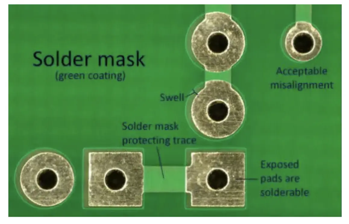
Solder mask misalignment refers to the improper positioning of the solder mask layer relative to the copper features on a PCB. The solder mask, a protective coating, is applied to prevent solder bridges and protect traces from environmental damage. When misalignment occurs, areas meant to be covered may be exposed, or openings intended for soldering may be partially blocked. This defect disrupts the PCB manufacturing process and can compromise the board's integrity.
The importance of precise solder mask registration cannot be overstated. Misalignment can lead to assembly failures, reduced product lifespan, and costly rework. For engineers working on high reliability applications such as aerospace or medical devices, even minor deviations can result in catastrophic outcomes. Adhering to industry standards like IPC-6012E ensures that solder mask application meets performance expectations, safeguarding the board against defects and ensuring consistent quality in production environments.
Causes of Solder Mask Misalignment in PCB Manufacturing
Understanding the root causes of solder mask misalignment is the first step toward mitigating this common PCB manufacturing defect. Several factors contribute to this issue during the production process.
Inaccurate Artwork or Gerber Files
The design phase sets the foundation for solder mask application. Errors in artwork or Gerber files, such as incorrect layer alignment or scaling issues, can lead to misalignment during manufacturing. If the digital representation of the solder mask does not match the copper layer precisely, the applied mask will be offset.
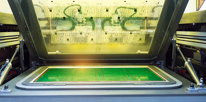
Equipment Calibration Issues
Manufacturing equipment used for solder mask application must be finely calibrated. Misaligned imaging systems or printing tools can cause the mask to be applied incorrectly. Over time, wear and tear on machinery may introduce subtle deviations that accumulate into significant registration errors.
Material Shrinkage or Expansion
PCBs are constructed from materials that can expand or contract due to temperature and humidity changes. During the solder mask curing process, if the substrate or mask material behaves unpredictably, it can shift relative to the copper features. This thermal mismatch often results in misalignment.
Human Error in Process Control
Manual handling or oversight during production can introduce errors. For instance, improper loading of panels into printing machines or incorrect setup of process parameters may lead to solder mask registration issues. Consistent training and adherence to protocols are vital to minimize such risks.
Panel Movement During Processing
During production of multilayer PCBs, panels are subjected to multiple processing steps. Any unintended movement or vibration during solder mask application can cause the layer to shift. Securing panels properly throughout the workflow is essential to prevent these deviations.
Consequences of Solder Mask Misalignment on PCB Performance
Solder mask misalignment can have far reaching effects on the functionality and reliability of a PCB. Electrical engineers must recognize these consequences to prioritize quality control measures.
Exposure of Copper Traces
When the solder mask does not cover copper traces as intended, these conductive areas become vulnerable to oxidation and environmental contaminants. Exposed traces can also lead to unintended solder bridges during assembly, causing short circuits.
Blocked or Partial Pad Openings
Misaligned solder mask may partially cover pads meant for component soldering. This obstruction can prevent proper solder joint formation, leading to weak connections or complete assembly failures. Such defects are particularly problematic in surface mount technology applications.
Reduced Insulation Properties
The solder mask serves as an insulating layer. Misalignment compromises this protection, increasing the risk of electrical leakage between adjacent traces. In high voltage applications, this can result in arcing or catastrophic board failure.
Increased Rework and Production Costs
Detecting and correcting solder mask misalignment often requires additional inspection and rework. This not only delays production schedules but also raises costs. In severe cases, entire batches may need to be scrapped, impacting profitability.
Compliance Issues with Standards
Misalignment can cause a PCB to fail acceptance criteria outlined in standards such as IPC-A-600K. Non compliance may lead to rejection by clients or regulatory bodies, especially in industries requiring strict adherence to quality specifications.
Practical Solutions for Preventing Solder Mask Misalignment
Addressing solder mask misalignment requires a combination of design diligence, process optimization, and quality control. Below are actionable strategies for electrical engineers and manufacturing teams.
Optimize Design Files for Precision
Ensure that design files are meticulously prepared with accurate layer alignment. Use design rule checks to verify solder mask registration against copper features. Following guidelines from standards like IPC-6012E helps in setting appropriate tolerances for mask clearance and coverage.
Regular Equipment Maintenance
Implement a strict maintenance schedule for imaging and printing equipment. Routine calibration checks can detect and correct deviations before they impact production. Automated systems with feedback mechanisms can further enhance precision during solder mask application.
Control Environmental Conditions
Maintain stable temperature and humidity levels in the manufacturing facility to minimize material expansion or shrinkage. Adhering to process controls outlined in standards such as ISO 9001:2015 ensures consistency across production runs and reduces variability.
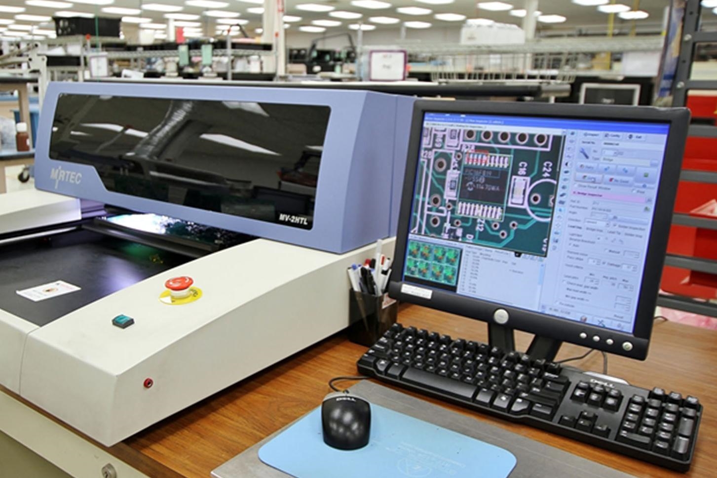
Implement Automated Optical Inspection
Automated optical inspection systems can detect solder mask misalignment early in the process. These tools compare the applied mask against design specifications, identifying deviations with high accuracy. Integrating such checks into the workflow strengthens PCB quality control.
Enhance Operator Training
Provide comprehensive training for personnel involved in solder mask application. Emphasize the importance of proper panel handling and process adherence. Regular audits of operator performance can identify areas for improvement and reduce human error.
Suggested Reading: Understanding Solder Mask: A Beginner's Guide to PCB Protection
Best Practices for Solder Mask Registration in High Reliability Applications
For applications demanding the highest reliability, additional measures can ensure precise solder mask registration. Electrical engineers working on such projects should consider the following.
- Tighten Design Tolerances: Work with narrower tolerances for solder mask clearance, as specified in IPC-A-600K, to account for potential shifts during manufacturing.
- Use Fiducial Marks: Incorporate fiducial marks on PCB panels to guide alignment during solder mask application. These reference points improve registration accuracy.
- Select High Quality Materials: Choose solder mask materials with known thermal stability to reduce the risk of shrinkage or expansion during curing.
- Conduct Pilot Runs: Perform small scale production runs to validate process parameters before full scale manufacturing. This approach helps identify potential issues early.
Troubleshooting Solder Mask Misalignment in Production
When misalignment occurs, a systematic approach to troubleshooting can minimize downtime and prevent recurrence. Start by reviewing design files for discrepancies in layer alignment. Inspect equipment logs to check for calibration issues or anomalies during the application process. Analyze environmental data to rule out thermal or humidity related shifts. Finally, use inspection tools to pinpoint the extent of misalignment and determine if rework is feasible. Documenting findings and corrective actions ensures continuous improvement in PCB manufacturing processes.
Conclusion
Solder mask misalignment poses significant challenges in PCB manufacturing, affecting both performance and reliability. By understanding the causes, such as design errors, equipment issues, and material behavior, engineers can implement targeted solutions to enhance solder mask registration. Strategies like optimized design preparation, regular equipment maintenance, and automated inspection play a crucial role in maintaining PCB quality control. Adherence to industry standards ensures that production meets stringent requirements, delivering robust boards for critical applications. Through proactive measures and systematic troubleshooting, manufacturers can mitigate the risks of solder mask misalignment and achieve consistent, high quality results.
FAQs
Q1: What are the primary causes of solder mask misalignment in PCB manufacturing?
A1: Solder mask misalignment often results from inaccurate design files, equipment calibration issues, or material expansion during processing. Poor panel handling and environmental variations also contribute to this defect. Ensuring precise design alignment and maintaining stable production conditions, as guided by standards like IPC-6012E, can significantly reduce these risks during PCB manufacturing.
Q2: How does solder mask misalignment impact PCB quality control?
A2: Misalignment compromises PCB quality control by exposing copper traces or blocking solder pads, leading to short circuits or weak connections. This can cause failures in assembly and operation. Regular inspections and adherence to standards like IPC-A-600K are essential to detect and address such issues, ensuring the board meets reliability expectations.
Q3: What solutions can improve solder mask registration in production?
A3: Improving solder mask registration involves optimizing design files, calibrating equipment regularly, and controlling environmental factors. Automated optical inspection systems help detect errors early. Following guidelines from ISO 9001:2015 for process consistency and using fiducial marks for alignment can further enhance precision in solder mask application.
Q4: Why is solder mask application critical for high reliability PCBs?
A4: Solder mask application is vital for high reliability PCBs as it protects traces and prevents solder bridges in critical applications. Misalignment can lead to electrical failures or insulation loss. Strict adherence to standards like IPC-6012E during application ensures the mask performs its protective role effectively, maintaining board integrity.
References
IPC-6012E — Qualification and Performance Specification for Rigid Printed Boards. IPC, 2020.
IPC-A-600K — Acceptability of Printed Boards. IPC, 2020.
ISO 9001:2015 — Quality Management Systems. ISO, 2015.


