Introduction
Manual PCB cleaning after rework stands as a critical final step in ensuring assembly reliability. Rework processes, such as component replacement or solder joint repair, often introduce flux residues, solder particles, and contaminants that compromise electrical performance if left unaddressed. Electric engineers frequently encounter these challenges in prototyping, repair stations, or high-mix production environments where automated cleaning systems prove impractical. This guide outlines the manual PCB cleaning process with precision, focusing on best practices for manual cleaning to achieve contamination-free boards. By following structured techniques, engineers can prevent issues like dendritic growth or signal degradation. Proper execution aligns with industry expectations for durable, high-performance electronics.
Why Manual PCB Cleaning After Rework Matters
Flux residues from rework soldering activate under humidity and voltage, leading to ionic migration that forms conductive paths between traces. Even no-clean fluxes can become problematic post-rework due to thermal stress altering their chemistry. Contaminants trap moisture, accelerating corrosion on copper features or promoting electromigration in fine-pitch components. In mission-critical applications, unclean boards fail premature reliability tests, increasing field returns and costs. The manual PCB cleaning process restores surface integrity, enabling consistent insulation resistance and visual acceptability. Engineers prioritizing this step extend product lifespan and meet compliance thresholds without relying on capital-intensive equipment.
Neglecting cleaning introduces troubleshooting nightmares, such as intermittent shorts or leakage currents during burn-in. Standards like IPC J-STD-001 emphasize post-rework cleanliness to verify residue removal. This practice proves essential in environments demanding quick turnaround, where manual methods offer control and immediacy. Ultimately, thorough cleaning safeguards signal integrity across high-speed interfaces and power planes.
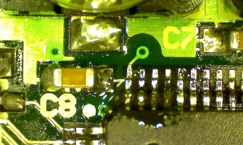
Understanding Contaminants from Rework and Their Effects
Rework introduces multiple contaminant types, including activated flux rosin, halide salts from aggressive fluxes, and particulate matter like solder splatter. These adhere to pads, vias, and under components, creating hidden traps difficult to access. Soluble residues dissolve slowly in solvents, while particulates embed mechanically, requiring agitation for dislodgement. Exposure to elevated temperatures during rework volatilizes some flux but leaves hygroscopic films that attract ambient moisture. Such films lower surface insulation resistance, fostering failures in humid conditions or under bias.
Mechanical damage from rework tools exacerbates contamination risks, with exposed laminate fibers acting as wicks for residues. Engineers observe these effects through white residue corrosion or bridging in densely populated boards. Proper identification precedes effective cleaning, often via visual inspection or scope examination. Addressing these mechanisms ensures the board meets performance specs post-cleaning.
Selecting Materials for the Manual PCB Cleaning Process
Choose solvents based on flux classification: alcohol for rosin-based, water with surfactants for aqueous types, avoiding incompatibles that swell solder masks. Isopropyl alcohol at high purity suits most manual applications due to fast evaporation and low residue. Lint-free swabs, nylon brushes with soft bristles, and microfiber wipes form the core toolkit for precise application. ESD-safe gloves and static-dissipative mats prevent charge buildup during handling. Compressed air or low-pressure nitrogen aids drying without static generation.
Compatibility testing on scrap material confirms no delamination or trace attack. Engineers stock multiple brush sizes for tight spaces around QFNs or BGAs. Material selection influences cleaning efficacy, with improper choices leading to smearing or incomplete removal.
Step-by-Step Manual PCB Cleaning Process
Step 1: Preparation and Safety Setup
Begin in a well-ventilated area with fume extraction to handle solvent vapors safely. Don ESD-safe attire and ground the workstation to protect sensitive components. Perform initial inspection under 10x magnification to map residue locations, noting heavy flux zones near reworked joints. Mask adjacent areas if aggressive solvents risk nearby features. Secure the PCB on a flat, non-conductive surface to prevent flexing during cleaning. This setup minimizes secondary contamination and operator hazards.
Step 2: Gross Debris Removal
Use low-pressure compressed air to dislodge loose solder balls and fibers before solvent contact. Gently tilt the board to avoid propelling particles into crevices. A soft vacuum pickup removes stubborn particulates without scratching traces. Avoid high-velocity blasts that embed debris deeper. This initial pass prepares surfaces for targeted solvent work, aligning with best practices for manual cleaning.
Step 3: Solvent Application Techniques
Saturate lint-free swabs sparingly with solvent, applying in one-directional strokes from clean to dirty areas. For broad surfaces, use a soft nylon brush dipped lightly, working flux into solution without flooding vias. Focus on reworked sites, circling pads and joints methodically. Renew swabs frequently to prevent residue redeposition. These solvent application techniques ensure thorough dissolution without pooling, which could wick under components.
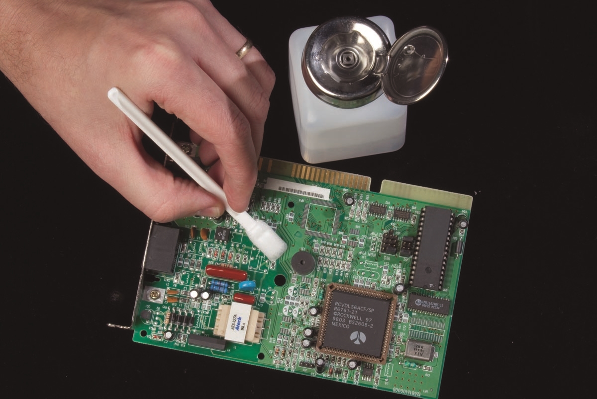
Step 4: Using Brushes and Swabs for PCB Cleaning
Select fine-tip swabs for precision around pins and under low-profile parts, twisting gently to lift residues. Nylon brushes excel on flat pads, with short, feathering strokes minimizing abrasion. Alternate tools per zone: swabs for crevices, brushes for open areas. Monitor solvent saturation to maintain wet cleaning action until flux clarifies. Best practices for manual cleaning dictate tool changes every few passes to sustain cleanliness.
Troubleshoot brush marks by switching to softer bristles or reducing pressure. This targeted approach handles varied geometries effectively.
Step 5: Rinsing and Residue Verification
Follow initial cleaning with a fresh solvent pass or deionized water rinse for water-soluble fluxes, using swabs to capture dissolved contaminants. Inspect under white light and UV if fluorescent tracers aid visibility. Black light reveals halide residues glowing distinctly. Verify no standing liquid or streaks remain. IPC-7711/7721 procedures guide these verification steps for rework reliability.
Step 6: Drying and Final Inspection
Air dry vertically in a laminar flow hood or use filtered nitrogen to evaporate solvents rapidly. Bake at low temperature if aqueous cleaning occurred, ensuring complete moisture expulsion. Re-inspect under magnification for residue remnants, checking IPC-A-610 criteria for acceptability. Document findings with photos for traceability. Proper drying prevents hydration-induced failures.
Best Practices for Manual Cleaning and Common Pitfalls
Adhere to minimal solvent volumes to avoid capillary action drawing flux deeper. Clean promptly post-rework, within hours, as residues harden over time. Train operators on consistent pressure to prevent solder mask scratches. Rotate cleaning directions to dislodge embedded particles effectively. Integrate ionic contamination testing where feasible, per J-STD-001 guidelines.
Avoid pitfalls like over-saturation causing bridging or using contaminated wipes redepositing debris. Engineers troubleshoot incomplete cleaning by revisiting shadowed areas under components with angled swabs. Document process variations for continuous improvement.
Troubleshooting Issues in Manual PCB Cleaning
Persistent white residues signal incompatible solvents; switch to higher polarity options and extend dwell time. Smeared flux indicates excessive pressure; lighten touch and use fresh tools. Post-clean corrosion points to incomplete drying; extend bake cycles or improve airflow. Shadowed contamination under parts requires flexible extension swabs or localized ultrasonics if manual limits reached. Static damage appears as charred components; enhance grounding protocols.
Case in point: A high-density board with BGA rework showed leakage after cleaning; root cause was unrinsed solvent in vias, resolved by extended nitrogen purge. Systematic diagnosis preserves rework investments.
Conclusion
Mastering the manual PCB cleaning process after rework demands attention to preparation, precise tool use, and rigorous verification. Best practices for manual cleaning, including using brushes and swabs for PCB cleaning and solvent application techniques, yield boards free of performance-robbing contaminants. Engineers applying these steps enhance reliability, reduce defects, and align with standards like IPC J-STD-001. Consistent execution turns rework from risk to routine, supporting demanding electronic applications.
FAQs
Q1: What are the key steps in the manual PCB cleaning process after rework?
A1: The process starts with safety setup and debris removal using air, followed by solvent application with swabs and brushes on targeted areas. Rinse if needed, dry thoroughly with nitrogen, and inspect under magnification per IPC J-STD-001. This ensures flux residues and particulates vanish without damage. Focus on one-directional strokes for efficiency.
Q2: Why prioritize best practices for manual cleaning in rework scenarios?
A2: Best practices prevent ionic migration and corrosion by removing all residues promptly. Techniques like minimal solvent use avoid wicking issues, while tool rotation maintains efficacy. They align with IPC-7711/7721 for reliable repairs. Skipping them risks shorts in humid environments.
Q3: How effective are using brushes and swabs for PCB cleaning under components?
A3: Brushes handle open pads with feathering strokes, while swabs excel in tight spaces like QFN gaps, twisting to lift flux. Renew frequently to prevent smearing. These tools enable precise access without automated gear, ideal for prototypes. Verify with UV light for completeness.
Q4: What solvent application techniques optimize residue removal?
A4: Apply sparingly in clean-to-dirty directions, saturating tools not boards to control flow. Dwell briefly for dissolution, then wipe. Compatible solvents like high-purity IPA suit most fluxes. This minimizes pooling and ensures even cleaning across varied surfaces.
References
IPC J-STD-001G — Requirements for Soldered Electrical and Electronic Assemblies. IPC, 2017
IPC-7711/7721C — Rework, Repair and Modification of Electronic Assemblies. IPC, 2018
IPC-A-610H — Acceptability of Electronic Assemblies. IPC, 2019


