Introduction
High-frequency PCBs operate at signal speeds exceeding several gigahertz, where even minor imperfections can degrade performance and lead to system failures. PCB testing becomes critical to verify material properties, trace integrity, and overall reliability in applications like telecommunications, radar systems, and high-speed data processing. High-frequency PCB testing focuses on parameters such as signal integrity, controlled impedance, and minimal losses to prevent issues like crosstalk and reflections. Engineers must employ precise measurement techniques to ensure these boards meet stringent quality standards before deployment. This article explores key testing methods, their principles, and best practices for achieving optimal results. By understanding these techniques, electric engineers can enhance design validation and manufacturing outcomes.
Challenges in High-Frequency PCB Testing
High-frequency signals propagate as electromagnetic waves along PCB traces, making them susceptible to dielectric losses, conductor skin effect, and radiation. These factors demand specialized PCB testing beyond standard low-frequency checks, as conventional methods may overlook subtle discontinuities. Impedance mismatches, for instance, cause signal reflections that distort waveforms and reduce eye diagram margins. Thermal expansions during operation can also warp boards, affecting via reliability and alignment. Factory-driven insights emphasize early detection through standardized procedures to minimize rework costs. Addressing these challenges ensures compliance with performance specifications and extends product lifespan.
Key Principles of Signal Integrity Testing
Signal integrity testing evaluates how well high-frequency signals maintain their shape from transmitter to receiver on a PCB. Core principles involve measuring insertion loss, return loss, and crosstalk using vector network analyzers or time-domain methods. At gigahertz frequencies, the PCB acts as a transmission line, where characteristic impedance must remain consistent to avoid reflections governed by the reflection coefficient formula. Dielectric materials with low dissipation factors are essential, but manufacturing variations like plating thickness can alter effective impedance. Engineers analyze S-parameters to quantify these effects, ensuring the board supports data rates without errors. Structured testing protocols align with industry methods for repeatable results.
Flying Probe Testing for Electrical Verification
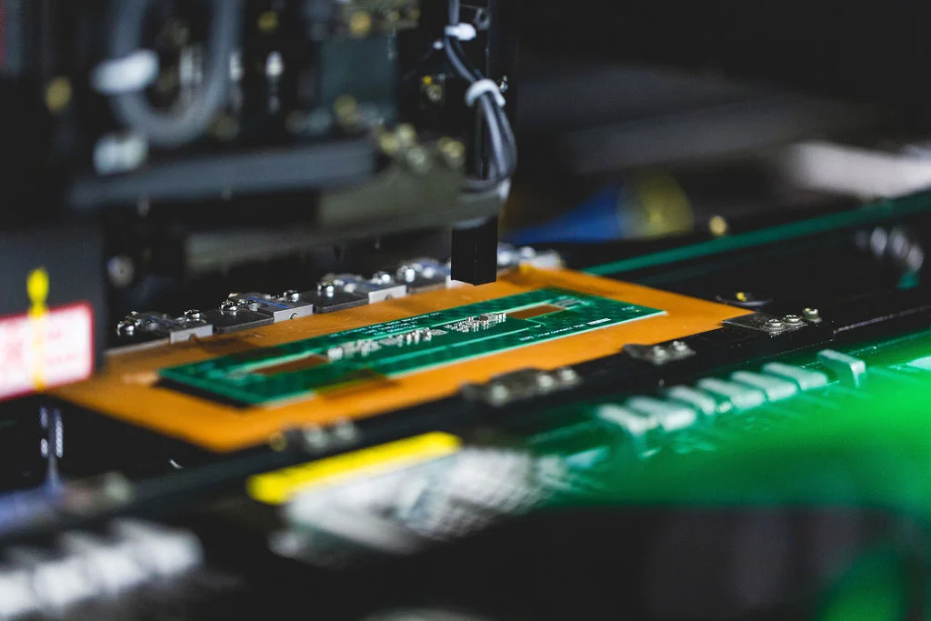
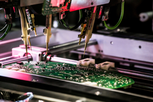
Flying probe testing uses automated probes that move across the PCB surface to check continuity, shorts, and resistance without fixtures. This method excels for prototypes and low-volume high-frequency PCBs, where bed-of-nails testers prove impractical due to fine-pitch nets. Probes make sequential contact at test points, applying low-voltage signals to detect opens or insulation failures as low as megohms. In high-frequency contexts, it verifies netlist integrity before advanced measurements, catching assembly defects early. The technique supports double-sided access and adapts to irregular geometries common in RF boards. Factory practices integrate flying probe testing post-fabrication to confirm electrical functionality prior to signal integrity checks.
Impedance Measurement Techniques
Impedance measurement quantifies the characteristic impedance of traces and vias, crucial for matching source and load in high-frequency designs. Techniques include time-domain reflectometry and frequency-domain analysis, each offering complementary insights. Engineers calculate impedance from trace width, thickness, dielectric height, and material constants using established formulas. Variations beyond tolerances, often 10% or tighter, lead to signal degradation, necessitating precise control during lamination and etching. Test coupons embedded on panels provide representative samples for non-destructive evaluation. Consistent impedance ensures predictable signal propagation and minimizes the need for redesigns.
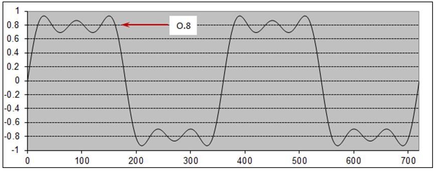
TDR Testing: Detecting Discontinuities
TDR testing sends a fast-rising step signal down a trace and measures reflections to map impedance profile along the line. Discontinuities like vias, bends, or etch variations appear as impedance steps on the oscilloscope trace, allowing pinpoint location via time-to-distance conversion. This method, detailed in IPC-TM-650 2.5.5.7, supports resolutions down to millimeters, ideal for high-frequency PCB testing. Rise times below 50 picoseconds enable accurate profiling up to tens of gigahertz. Engineers interpret waveforms to quantify mismatches, such as a 50-ohm line showing spikes at 60 ohms. Post-analysis, adjustments in routing or stackup optimize performance.
Advanced Signal Integrity Testing with VNAs
Vector network analyzers perform frequency-domain signal integrity testing by sweeping signals across a band and capturing S-parameters. Measurements reveal insertion loss from conductor and dielectric attenuation, critical for multi-gigabit links. Crosstalk assessment between adjacent traces identifies coupling risks, guiding spacing rules. Calibration with standards like short-open-load-thru ensures accuracy across connectors and fixtures. High-frequency PCB testing via VNAs validates eye patterns indirectly through equalization simulations. These insights inform iterative improvements in layer stackup and material selection.
Integrating Thermal and Mechanical Measurements
High-frequency PCBs endure thermal cycling, requiring warpage and CTE measurements to predict reliability. Dial gauges or laser interferometers quantify bow and twist per IPC-6012 specifications. Mechanical stress from vias and planes influences signal paths, so cross-sectioning reveals plating voids or cracks. Thermal imaging during powered testing detects hotspots from poor heat dissipation. Combining these with electrical tests provides a holistic quality view. Engineers use data to refine solder mask applications and via designs for robustness.
Best Practices for Comprehensive High-Frequency PCB Testing
Start with design verification using simulation tools to predict impedance and losses before fabrication. Incorporate test coupons for impedance, TDR, and coupon loss measurements on production panels. Sequence tests from visual inspection to flying probe, then advanced signal integrity checks. Maintain controlled environments to avoid humidity-induced variations in measurements. Document results against tolerances, tracing deviations to process steps like etching or lamination. Collaborate across design and manufacturing for feedback loops that enhance yield.
Regular calibration of equipment ensures traceability, while operator training upholds procedural consistency. For high-volume runs, hybrid flying probe and fixtureless methods scale efficiently. Post-assembly retesting verifies reflow impacts on impedance. These practices align with qualification standards, reducing field failures.
Troubleshooting Common Issues in High-Frequency Testing
Impedance deviations often stem from dielectric thickness inconsistencies, addressed by precise press cycles. TDR spikes at vias suggest stub lengths exceeding quarter-wavelength at operating frequency; shortening or back-drilling resolves this. Excessive insertion loss points to rough copper surfaces, mitigated by low-profile foils. Crosstalk failures require wider spacing or ground shielding. Flying probe opens may indicate mask registration errors. Systematic root-cause analysis, supported by IPC-TM-650 methods, guides corrective actions.
Conclusion
Effective testing and measurement techniques safeguard high-frequency PCBs against performance pitfalls, ensuring signal integrity and long-term reliability. From flying probe electrical checks to TDR and impedance measurements, each method contributes to a layered quality assurance strategy. Adhering to standards like IPC-6012 fortifies manufacturing processes. Electric engineers benefit from integrating these practices into workflows for superior outcomes. Ultimately, rigorous PCB testing translates to robust systems in demanding applications.
FAQs
Q1: What is TDR testing in high-frequency PCB testing?
A1: TDR testing employs time-domain reflectometry to detect impedance discontinuities by analyzing reflections from a step signal. It maps trace profiles with high resolution, identifying issues like vias or etch variations. This technique is vital for signal integrity testing, ensuring controlled impedance up to multi-gigahertz frequencies. Factories use it per standardized methods for precise fault location.
Q2: How does flying probe testing support PCB testing for prototypes?
A2: Flying probe testing automates electrical verification without custom fixtures, ideal for low-volume high-frequency prototypes. Probes check continuity, shorts, and resistance across fine nets efficiently. It precedes impedance measurement by confirming basic connectivity. This flexible approach minimizes setup time while maintaining quality.
Q3: Why is impedance measurement critical in signal integrity testing?
A3: Impedance measurement verifies trace consistency to prevent reflections that degrade high-frequency signals. Techniques like TDR quantify variations from design targets. Consistent impedance supports data integrity in RF applications. Engineers rely on it for stackup validation and process control.
Q4: What role does signal integrity testing play in high-frequency PCB reliability?
A4: Signal integrity testing assesses loss, crosstalk, and return loss to predict real-world performance. Tools like VNAs provide S-parameter data for simulations. It ensures boards handle gigabit speeds without errors. Comprehensive testing enhances overall PCB reliability.
References
IPC-TM-650 2.5.5.7 — Characteristic Impedance of Lines on Printed Boards by TDR. IPC.
IPC-6012E — Qualification and Performance Specification for Rigid Printed Boards. IPC, 2015.
IPC-2221B — Generic Standard on Printed Board Design. IPC, 2012.


