Introduction
Impedance control plays a critical role in modern PCB manufacturing, especially for high-speed designs where signal integrity directly impacts performance. Electrical engineers rely on precise impedance matching to minimize reflections, crosstalk, and losses in transmission lines. Testing and verification ensure that fabricated boards meet design specifications before assembly. This article explores PCB impedance testing methods, including Time-Domain Reflectometry (TDR) PCB testing and Vector Network Analyzer (VNA) PCB testing, along with impedance test coupon design. Factory processes emphasize standardized approaches to deliver reliable results. Understanding these techniques helps engineers collaborate effectively with manufacturers.
Without proper control, high-speed signals degrade rapidly over distance. Gigahertz frequencies demand tolerances as tight as +/-5% to +/-10%. Factories integrate testing into quality control workflows, reducing rework and field failures. Engineers specify requirements clearly to align manufacturing capabilities. Ultimately, robust impedance verification supports reliable system operation in telecommunications, computing, and automotive sectors.
What Is Impedance Control and Why It Matters
Impedance control refers to maintaining a consistent characteristic impedance along PCB traces, typically 50 ohms for single-ended lines or 100 ohms for differential pairs. Variations arise from factors like dielectric thickness, trace width, copper roughness, and material properties. In high-frequency applications, mismatches cause signal distortion, leading to bit errors or timing issues. Manufacturers verify impedance post-fabrication to confirm stackup accuracy and process stability. Compliance with standards like IPC-2221 ensures design-to-production fidelity. For electrical engineers, this verification bridges simulation and real-world performance.
Without proper control, high-speed signals degrade rapidly over distance. Gigahertz frequencies demand tolerances as tight as +/-5% to +/-10%. Factories integrate testing into quality control workflows, reducing rework and field failures. Engineers specify requirements clearly to align manufacturing capabilities. Ultimately, robust impedance verification supports reliable system operation in telecommunications, computing, and automotive sectors.
Technical Principles of Impedance Testing
Characteristic impedance derives from transmission line theory, where Z0 = sqrt(L/C) for lossless lines, with L as inductance and C as capacitance per unit length. In PCBs, microstrip and stripline configurations dominate, influenced by substrate epsilon_r and geometry. Testing measures effective impedance to validate these parameters. Two primary PCB impedance testing methods prevail: time-domain and frequency-domain approaches. Each suits specific scenarios based on resolution and frequency range needs.
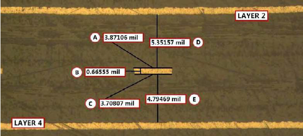
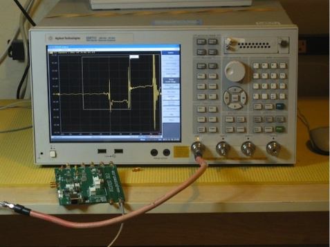
Time-Domain Reflectometry (TDR) PCB testing sends a fast-rise-time step signal along a trace and analyzes reflections. Discontinuities cause voltage steps proportional to impedance change via reflection coefficient rho = (Z2 - Z0)/(Z2 + Z0). Engineers interpret waveforms for average impedance, mismatches, or faults like voids. TDR excels in locating defects spatially, with resolutions down to millimeters depending on rise time. Factories prefer it for production due to speed and simplicity. Calibration against known standards ensures accuracy.
Vector Network Analyzer (VNA) PCB testing operates in the frequency domain, measuring S-parameters like S11 for return loss. Impedance is extracted from magnitude and phase data, often via TRL calibration for precision. VNA captures frequency-dependent effects, ideal for broadband analysis up to millimeter-wave. It reveals losses from skin effect or dielectric tan delta. While more comprehensive, VNA requires skilled operation and longer setup. Both methods complement each other in thorough verification.
Impedance Test Coupon Design
Impedance test coupons are dedicated structures on production panels, replicating critical trace geometries without interfering with circuitry. Placed at panel edges, they allow non-destructive probing post-plating and etching. Design per IPC-2221 guidelines includes straight traces of 100-150 mm length for stable measurements, avoiding bends that introduce errors. Single-ended, differential, and edge-coupled pairs cover common configurations. Vias or launch pads enable SMA connector attachment.
Coupon layout considers stackup layers, with multiple coupons verifying inner and outer layers separately. Engineers specify nominal impedance, tolerance, and test points in fab drawings. Factories etch coupons alongside product traces using identical processes for representativeness. Variations in copper weight or dielectric thickness affect all similarly. Poor design leads to measurement artifacts, so symmetry and isolation matter. Valid coupons confirm overall panel quality.
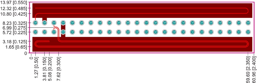
Optimal design minimizes parasitic effects. Ground planes mirror production routing. For multilayer boards, coupons span target layers. Post-fab, coupons undergo electrical test before panel routing. Rejected panels trigger process adjustments like lamination pressure or etch control. Engineers review coupon data alongside cross-sections for correlation.
Practical Implementation of TDR PCB Testing
TDR PCB testing begins with fixture preparation, launching the signal via coaxial adapters to coupon pads. Step generator rise time, typically 35-50 ps, determines spatial resolution via distance = (c * tr) / (2 * sqrt(epsilon_r)). Waveform displays voltage versus time, converted to distance and impedance scales. Factories set pass/fail based on spec bands, often +/-10%. Bulk average impedance integrates over length, while eye checks discontinuities.
Environmental factors like temperature affect measurements, so testing occurs at controlled 23°C. Pre-test cleaning removes residues impacting contact. Automated TDR systems scan multiple coupons rapidly. Data logs include waveforms and stats for traceability. Engineers analyze for trends, like dielectric thinning. Consistent results validate manufacturing repeatability.
Challenges include connector launch transitions adding ripple. De-embedding software corrects this. IPC-TM-650 method 2.5.5.7 standardizes TDR procedures for repeatability. Factories calibrate daily against air lines or shorts. This ensures metrology-grade accuracy.
VNA PCB Testing in Manufacturing
VNA PCB testing requires a full two-port setup for transmission, but single-ended reflection can suffice for impedance. Calibration kits with opens, shorts, loads, and thru establish the reference plane. Swept frequencies from DC to 20 GHz reveal resonances or losses. Smith chart or magnitude plots highlight deviations. Factories use VNA for qualification lots or high-reliability products.
Time-gating transforms frequency data to the time domain, mimicking TDR for fault location. This hybrid approach combines strengths. Higher cost limits routine use, but it verifies TDR findings. Engineers specify frequency range matching signal harmonics. Post-processing extracts effective epsilon_r and losses.
Integration with SPC monitors process drift. VNA suits complex structures like backplanes.
Best Practices for Verification in Manufacturing
Specify impedance early in design, providing stackup details and calculator models. Request coupons on all panels for 100% verification. Define tolerance realistically, considering material spreads. Factories cross-check with flying probe continuity pre-impedance test. Document deviations with root cause analysis.
Layer-to-layer alignment affects coupling; verify via coupons. For HDI boards, microvia stubs impact high frequencies. Post-lamination tests predict final values. Engineers audit supplier capabilities via qualification panels.
Multistage verification includes design review, process control, and final test. Train operators on artifacts like overshoot. Archive data for audits.
Troubleshooting Common Issues
Impedance too high signals thin dielectric or wide traces; low indicates opposite. Etch undercut from over-etch enlarges traces. Voids in lamination cause bumps in TDR. Copper roughness adds loss, visible in VNA insertion loss. Factories adjust developer chemistry or foil type.
Coupon failure prompts full panel scan. Cross-section analysis confirms electrical data. Process tweaks restore control.
Conclusion
Effective testing and verification of impedance control ensures PCB reliability in demanding applications. TDR and VNA methods, supported by thoughtful test coupon design, form the backbone of factory quality assurance. Adhering to standards like IPC-2221 and IPC-TM-650 delivers consistent outcomes. Electrical engineers benefit from partnering with capable manufacturers. Prioritizing these practices minimizes risks and optimizes performance.
FAQs
Q1: What are the main PCB impedance testing methods?
A1: PCB impedance testing methods include Time-Domain Reflectometry (TDR) for quick discontinuity detection and Vector Network Analyzer (VNA) for frequency-domain precision. TDR uses reflections from step signals to plot impedance profiles along traces. VNA measures S-parameters to derive broadband characteristics. Factories select based on speed and detail needs. Coupons enable representative sampling.
Q2: How does Time-Domain Reflectometry (TDR) PCB testing work in practice?
A2: TDR PCB testing launches a fast pulse into a test coupon and captures reflections to compute local impedance. Reflection coefficient reveals mismatches, with waveforms scaled to distance. Optimal rise times provide fine resolution for fault location. Manufacturing verifies against tolerance bands post-etch. This method aligns with IPC-TM-650 standards for reliability.
Q3: What is involved in impedance test coupon design?
A3: Impedance test coupon design replicates production traces on panel margins, per IPC-2221 guidelines. Lengths around 150 mm ensure accurate averages, with pads for probing. Include single-ended and differential pairs matching critical nets. Placement avoids process gradients. Factories test before shipping, confirming stackup integrity.
Q4: When should Vector Network Analyzer (VNA) PCB testing be used over TDR?
A4: VNA PCB testing suits high-frequency or lossy lines where TDR lacks resolution. It captures dielectric and conductor losses across bands. Use for qualification or troubleshooting complex effects. TDR handles production volume faster. Combine for comprehensive verification.
References
IPC-2221B — Generic Standard on Printed Board Design. IPC, 2012
IPC-TM-650 2.5.5.7 — Characteristic Impedance of Lines on Printed Boards by TDR. IPC
IPC-2141 — Design Guide for High-Speed Controlled Impedance Circuit Boards. IPC


