Introduction
Multilayer PCBs form the backbone of modern electronics, enabling complex circuitry in compact forms. As designs push toward higher densities, traditional through-hole vias often fall short, consuming valuable routing space and complicating signal paths. Blind and buried vias emerge as critical solutions, offering precise layer connections without penetrating the entire board thickness. These multilayer PCB vias enhance performance in applications from telecommunications to automotive systems. Mastering their implementation requires understanding both design and manufacturing intricacies. This article explores the principles, processes, and best practices for blind via manufacturing, buried via manufacturing, and PCB layer stackup optimization.
Understanding Blind and Buried Vias: Definitions and Importance
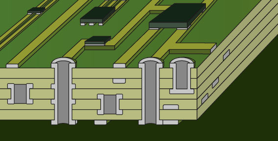
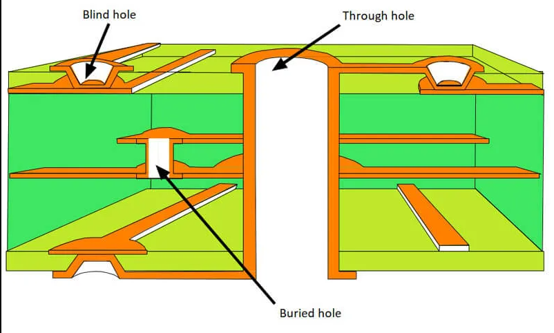
Blind vias connect an outer layer to one or more inner layers, stopping short of the opposite side to preserve surface real estate. Buried vias, in contrast, link exclusively inner layers, remaining invisible from both board surfaces. Together, these multilayer PCB vias enable tighter interconnects compared to standard through vias, which traverse all layers. Their adoption drives board miniaturization while maintaining electrical integrity. In high-density designs, they reduce parasitic capacitance and inductance, supporting faster signal speeds. Industry relevance grows with demands for smaller, more efficient devices across sectors like computing and medical equipment.
The distinction matters during PCB layer stackup planning, where via placement dictates routing efficiency. Without blind or buried options, designers face layer count increases or suboptimal traces. These vias align with reliability needs in harsh environments, minimizing stress points from thermal cycling. Factories prioritize them for advanced builds, ensuring compliance with qualification standards. Overall, they represent a shift from bulkier to streamlined architectures.
Technical Principles Behind Blind and Buried Vias
The core principle of blind and buried vias lies in controlled depth drilling relative to the PCB layer stackup. In a multilayer structure, cores—pre-laminated pairs of copper and dielectric—are drilled and plated before final assembly. This sequential approach allows vias to span specific layer pairs without affecting others. Electrical connectivity relies on electroless copper plating followed by electroplating, forming a robust barrel within the hole. Material compatibility between dielectrics and plating prevents delamination under mechanical stress.
Signal integrity benefits from shorter via stubs, as blind vias eliminate unused lengths that cause impedance mismatches. Buried vias further isolate inner signals from surface noise. Aspect ratios, defined as hole depth to diameter, influence plating uniformity and void risks. Factory processes control these to meet performance specs. Thermal management improves too, with targeted connections reducing heat spreading paths.
Blind Via Manufacturing: Step-by-Step Insights
Blind via manufacturing begins with core preparation, where mechanical or laser drilling creates precise depths. Mechanical methods suit larger diameters, punching through targeted layers post-lamination of select sub-stacks. Laser ablation excels for finer features, vaporizing dielectric without mechanical force. After drilling, desmear removes residue, ensuring clean walls for plating adhesion. Electroless seeding deposits initial copper, followed by pattern plating to build thickness.
Lamination integrates these cores into the full stackup, with prepregs bonding layers under heat and pressure. Registration accuracy proves vital, aligning vias across sub-stacks via fiducials. Final outer layer processing includes imaging and etching for surface traces. Inspection via cross-sectioning verifies depth and plating quality. This process demands tight process controls to avoid barrel cracks from expansion mismatches.
Sequential lamination cycles repeat for multiple blind vias, increasing complexity but enabling high-density interconnects. Factories sequence builds outward from inner cores, minimizing handling damage.
Buried Via Manufacturing: Precision Inner Layer Focus
Buried via manufacturing mirrors blind processes but confines operations to inner cores, invisible post-lamination. Drilling occurs on individual or paired cores before stacking, with plating completing the interconnect. This isolates buried vias from surface exposures, enhancing protection against environmental factors. Depth control relies on calibrated tooling, preventing over-drill into adjacent layers. Post-plating, cores undergo lamination, where alignment pins ensure positional integrity.
Unlike blind vias, buried ones avoid outer layer interactions, simplifying surface finishes. However, their fully encapsulated nature complicates rework, underscoring upfront design precision. Factories employ automated optical inspection during core stages to detect plating defects early. Thermal profiling during lamination prevents via protrusion or resin squeeze-out. Overall, buried via manufacturing boosts inner layer density without compromising outer usability.
IPC-6012 outlines qualification requirements for such multilayer boards with blind and buried vias, emphasizing plating integrity and dimensional stability.
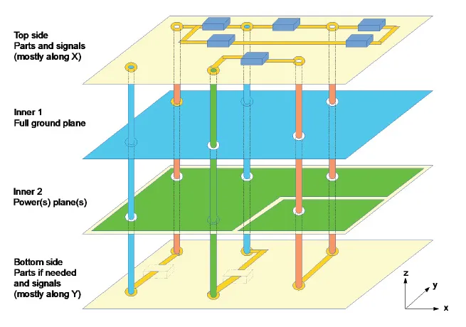
Optimizing PCB Layer Stackup for Multilayer PCB Vias
Effective PCB layer stackup planning integrates blind and buried vias from the outset, balancing signal, power, and ground layers. Designers map via spans to minimize transitions, grouping signals by net for efficiency. Core thickness dictates feasible depths, with thinner cores favoring laser vias. Symmetry in stackup prevents warpage, distributing copper weights evenly. Simulation tools verify impedance across via structures pre-manufacture.
Power integrity benefits from buried vias dedicating inner planes without surface clutter. Thermal vias can incorporate blind types for heat dissipation to inner planes. Factory feedback refines stackups, adjusting dielectric constants for controlled propagation. Aspect ratio guidelines cap depths to ensure reliable plating. Final stackups document via types per layer pair, aiding fabrication.
Best Practices for Reliable Via Implementation
Adhere to design rules like minimum via diameters and clearances, scaled to layer counts. Stagger vias across stackups to distribute stresses, avoiding clustered drilling. Select materials with matched CTEs between copper and dielectrics to mitigate cycling failures. IPC-2221 provides generic guidelines for via sizing and spacing in multilayer designs.
Plating thickness uniformity demands robust processes, often verified via microsection analysis. For high-reliability apps, tenting or filling protects vias per IPC-4761 via protection standards. Prototype iterations confirm manufacturability before volume runs. Collaborate early with fabricators on capabilities.
Common Challenges and Troubleshooting in Via Production
Warpage arises from asymmetric stackups or CTE mismatches, addressed by balanced layering. Plating voids stem from poor desmear, resolved via plasma treatment enhancements. Registration errors misalign vias, mitigated by advanced imaging systems. Electromigration risks in fine vias call for wider traces or filled structures.
Factory-driven solutions include process monitoring at each lamination cycle. Cross-section sampling catches issues early, correlating to IPC acceptance criteria. Adjusting drill parameters counters smear in high-aspect holes.
Conclusion
Blind and buried vias transform multilayer PCB design, enabling denser, higher-performing boards through targeted layer connections. From precise manufacturing sequences to thoughtful stackup planning, their mastery hinges on integrated engineering and production knowledge. Key to success lies in standards compliance, process control, and iterative validation. Engineers leveraging these multilayer PCB vias unlock compact innovations while upholding reliability. As demands escalate, proficiency in blind via manufacturing, buried via manufacturing, and PCB layer stackup remains essential.
FAQs
Q1: What distinguishes blind vias from buried vias in multilayer PCB vias?
A1: Blind vias link an outer layer to inner ones, visible on one surface, while buried vias connect only inner layers, hidden entirely. Both save space over through vias but require sequential lamination for precision. This setup optimizes routing in dense designs, aligning with factory processes for high yields. Proper stackup planning ensures compatibility.
Q2: How does blind via manufacturing impact PCB layer stackup choices?
A2: Blind via manufacturing involves depth-controlled drilling on sub-stacks, influencing core thicknesses and layer pairing. Thinner cores support finer vias, but demand symmetric builds to avoid warpage. Engineers plan stackups to match via spans, enhancing density without excess layers. Standards guide aspect ratios for plating reliability.
Q3: What are key steps in buried via manufacturing?
A3: Buried via manufacturing drills and plates inner cores before full lamination, ensuring isolated connections. Desmear, plating, and alignment precede pressing with prepregs. Inspection confirms integrity without surface exposure. This method boosts inner density, critical for complex multilayer PCB vias.
Q4: Why prioritize PCB layer stackup in blind and buried via designs?
A4: PCB layer stackup dictates via feasibility, affecting impedance, thermal paths, and warpage risks. Balanced arrangements with matched materials support reliable blind and buried vias. Early optimization prevents manufacturing hurdles, enabling high-density interconnects efficiently.
References
IPC-6012E — Qualification and Performance Specification for Rigid Printed Boards. IPC, 2017
IPC-2221B — Generic Standard on Printed Board Design. IPC, 2016
IPC-4761 — Via Protection and Covering Requirements. IPC, 2020


