Introduction
Plasma etching has emerged as a key process in printed circuit board manufacturing, offering significant advantages for creating sustainable PCBs. Traditional methods often rely on harsh chemical solutions that generate substantial waste and pose environmental risks. In contrast, plasma etching provides a dry, chemical-free PCB etching approach that aligns with the growing demand for green PCB production. This technique minimizes hazardous byproducts while maintaining high precision for multilayer boards and fine features. Factories adopting plasma etching report improved compliance with environmental regulations and reduced operational liabilities. As the electronics industry pushes toward eco-friendly etching, understanding plasma's role becomes essential for engineers optimizing production lines.
What Is Plasma Etching in PCB Manufacturing?
Plasma etching involves generating a low-pressure plasma from gases such as oxygen or argon to remove material from PCB surfaces through physical and chemical reactions. In PCB fabrication, it primarily serves desmear operations after drilling, where drill smear must be cleared for reliable plating adhesion. Unlike wet chemical desmear using permanganate solutions, plasma etching uses ionized gas radicals to etch away resin residues without liquids. This process ensures uniform surface preparation across panels, critical for high-density interconnects.
The relevance to sustainable PCB manufacturing lies in its ability to replace liquid-based processes that contribute to chemical waste streams. Engineers value plasma etching for its controllability, allowing adjustment of etch rates via power, gas flow, and pressure parameters. It supports compliance with IPC-6012E standards for rigid printed boards, where clean via walls are required for performance qualification. Overall, plasma etching integrates seamlessly into modern fabs aiming for reduced waste and eco-friendly etching.
Technical Principles of Plasma Etching
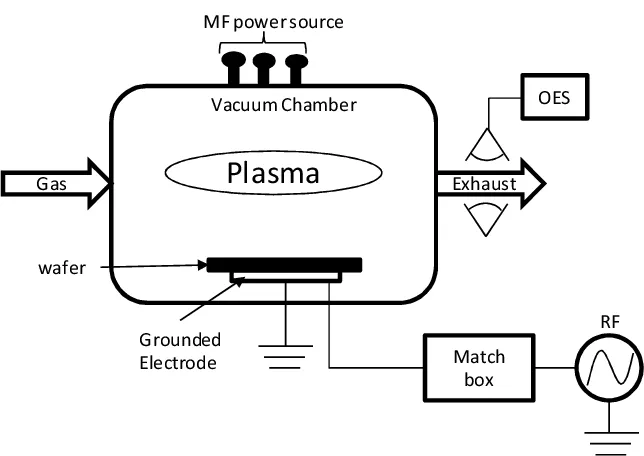
Plasma forms when radiofrequency energy excites process gases into a state of ionized particles, including electrons, ions, and reactive neutrals. These species bombard the PCB surface, breaking polymer bonds in epoxy smear and volatilizing residues as gaseous byproducts. Etch selectivity depends on gas chemistry; oxygen plasmas favor organic removal, while fluorinated gases enhance inorganic cleaning. Vacuum chambers maintain pressures around 0.1 to 1 Torr to sustain the glow discharge.
In PCB contexts, reactive ion etching variants combine chemical etching with physical sputtering for deeper desmear. Process uniformity is achieved through rotating electrode configurations or showerhead gas distribution, preventing over-etching on sensitive copper lands. Engineers monitor endpoints via optical emission spectroscopy to halt etching precisely. This precision supports green PCB goals by avoiding excess energy use or incomplete cleaning that necessitates rework.
Environmental Benefits of Plasma Etching
One primary advantage in the plasma etching environment is the elimination of wet chemistry, drastically cutting hazardous waste generation. Traditional permanganate desmear produces spent solutions laden with manganese sludge and organics, requiring neutralization and disposal. Plasma processes exhaust benign gases vented through abatement systems, aligning with chemical-free PCB etching ideals. Factories benefit from smaller footprints, as plasma units occupy less space than chemical tanks and rinse lines.
Water consumption drops significantly, since no rinsing follows plasma treatment. Chemical etching demands copious deionized water for neutralization and effluent dilution, straining resources in water-scarce regions. Plasma etching supports sustainable PCB initiatives by conserving this utility, indirectly lowering energy for water treatment. Compliance with ISO 14001:2015 environmental management systems becomes straightforward, as processes generate minimal effluents.
Air emissions are managed effectively, with plasma byproducts like CO2 and water vapor far less toxic than chemical vapors. Fluorine-based plasmas can be abated to prevent greenhouse gas release, further enhancing the plasma etching environment. Worker safety improves without exposure to corrosives, reducing personal protective equipment needs and health risks.
Energy efficiency varies but often favors plasma for batch processing, where rapid cycles offset RF power draw. Lifecycle assessments highlight lower overall impacts when factoring disposal savings. These factors position plasma etching as a cornerstone of green PCB manufacturing.
Plasma Etching Versus Traditional Chemical Etching
Chemical etching, dominant in panel processing, uses ferric chloride or cupric solutions that etch copper patterns but generate metal-laden sludge. Desmear specifically employs alkaline permanganate, followed by acid neutralization, creating multi-stage waste. Plasma etching targets desmear selectively, preserving copper integrity while avoiding these streams. Environmental footprints differ markedly, with plasma offering reduced waste across the board.
Precision in feature control favors plasma for advanced nodes, minimizing undercuts that lead to scrap. Chemical methods struggle with aspect ratios above 10:1, often requiring aggressive etches that increase material loss. Plasma's anisotropic nature ensures vertical smear removal without lateral spread. This efficiency translates to higher yields and less raw material waste in sustainable PCB production.
Cost analyses reveal long-term savings from plasma, despite higher equipment upfronts. Chemical handling incurs ongoing expenses for reagents, treatment, and permits. Plasma shifts costs to electricity and gases, scalable for high-volume fabs. Engineers transitioning processes note faster throughput, aiding eco-friendly etching adoption.
Best Practices for Implementing Plasma Etching
Select plasma systems with robust vacuum pumps and gas delivery for consistent etch rates. Calibrate recipes per laminate type, as FR-4 versus high-Tg materials respond differently. Pre-treat panels to remove gross contaminants, ensuring plasma focuses on smear. Monitor chamber cleanliness to prevent particle contamination, per IPC-A-600K acceptability criteria.
Integrate plasma into the drill-plating workflow post-hole inspection, targeting 75 microns minimum smear removal for plating adhesion. Use endpoint detection to optimize cycles, conserving energy. Vent exhaust through scrubbers for fluorine processes, maintaining plasma etching environment integrity. Train operators on safety interlocks and maintenance schedules.
For sustainable PCB lines, pair plasma with lead-free finishes and halogen-free laminates. Validate surface roughness via profilometry to confirm IPC-6012E compliance. Scale batch sizes to match production volumes, maximizing utilization. These practices ensure reliable, green PCB output.
Challenges and Solutions in Plasma Etching
Uniformity challenges arise in large panels, addressed by multi-zone RF power or planetary motion. Over-etching risks delicate structures, mitigated by low-power oxygen recipes. Gas selection balances speed and selectivity; argon adds sputtering for tough smears. Factory insights emphasize recipe qualification via cross-sections.
Cost barriers for small runs favor hybrid approaches, using plasma selectively for high-reliability boards. Maintenance downtime is minimized with modular designs. Engineers troubleshoot via plasma diagnostics, correlating etch depth to via performance.
Conclusion
Plasma etching revolutionizes PCB manufacturing by delivering eco-friendly etching with reduced waste and chemical-free operations. It supports sustainable PCB goals through lower water use, minimal effluents, and precise processing. Factories gain environmental compliance alongside performance gains, as seen in cleaner surfaces meeting industry benchmarks. As demand for green PCBs rises, plasma etching stands as a proven path forward for responsible production.
FAQs
Q1: What are the main environmental benefits of plasma etching in PCB manufacturing?
A1: Plasma etching reduces hazardous waste by eliminating wet chemicals used in traditional desmear, promoting a cleaner plasma etching environment. It cuts water usage since no rinsing is needed, and generates gaseous byproducts easily abated. This supports sustainable PCB production with lower disposal costs and regulatory burdens, ideal for factory efficiency.
Q2: How does plasma etching contribute to green PCB initiatives?
A2: As a chemical-free PCB etching method, plasma minimizes toxic effluents and worker exposure risks. It aligns with eco-friendly etching by conserving resources and space in fabs. Engineers achieve uniform desmear for reliable plating, enhancing overall green PCB yields without compromising quality.
Q3: Is plasma etching more sustainable than chemical etching for PCBs?
A3: Yes, plasma etching produces far less waste than chemical methods, which generate sludge and require extensive treatment. Reduced waste and no liquid effluents make it superior for the plasma etching environment. Factories report lower environmental liabilities, supporting long-term sustainable PCB manufacturing.
Q4: What role does plasma etching play in reduced waste PCB processes?
A4: Plasma etching excels in desmear, volatilizing residues without chemical residues or sludge. This directly lowers waste volumes compared to permanganate treatments. Integration fosters reduced waste practices, enabling compliance with standards while advancing eco-friendly etching in high-volume production.
References
IPC-6012E — Qualification and Performance Specification for Rigid Printed Boards. IPC, 2018
IPC-A-600K — Acceptability of Printed Boards. IPC, 2020
ISO 14001:2015 — Environmental Management Systems. ISO, 2015


