Introduction
Silkscreen layers on printed circuit boards serve as critical visual aids for component identification, assembly guidance, and regulatory compliance. In Altium Designer, these layers enable electric engineers to add text, symbols, outlines, and graphics directly onto the PCB layout. Proper silkscreen design enhances manufacturability, reduces assembly errors, and supports debugging during prototyping and production. This guide covers Altium silkscreen layer setup, creating silkscreen markings in Altium, and importing logos into Altium silkscreen, providing structured steps and engineering rationale. Engineers benefit from integrating silkscreen early in the design flow to align with fabrication capabilities. Mastering these techniques ensures boards meet functional and traceability requirements.
What Is PCB Silkscreen and Why It Matters
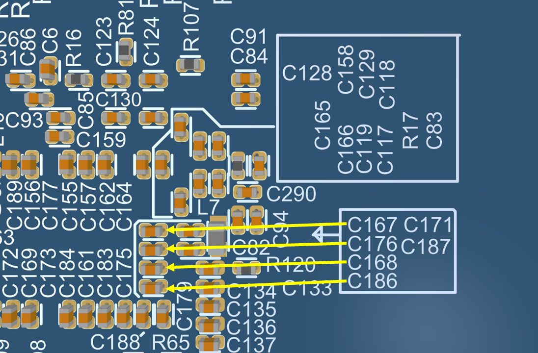
PCB silkscreen refers to the printed ink layer applied to the top and bottom surfaces of a board, typically using epoxy or UV-curable materials. It includes reference designators, polarity indicators, component outlines, part numbers, and logos, all placed on dedicated overlay layers in design software. This layer does not conduct electricity but provides essential human-readable information for operators during assembly, testing, and repair. Without clear silkscreen, errors like component misalignment or incorrect polarity increase, leading to yield losses. In high-reliability applications, silkscreen supports traceability back to manufacturing lots. Compliance with industry norms ensures legibility under various lighting and inspection conditions.
Silkscreen matters because it bridges design intent with physical production. Electric engineers rely on it for pin-1 orientation on ICs, voltage warnings, and connector pinouts, preventing field failures. During rework, technicians use markings to locate test points or fiducials quickly. Fabricators appreciate designs that minimize overlaps with pads or vias, simplifying printing processes. Overall, thoughtful silkscreen design streamlines the entire PCB lifecycle from schematic to deployment.
Silkscreen Layers in Altium Designer
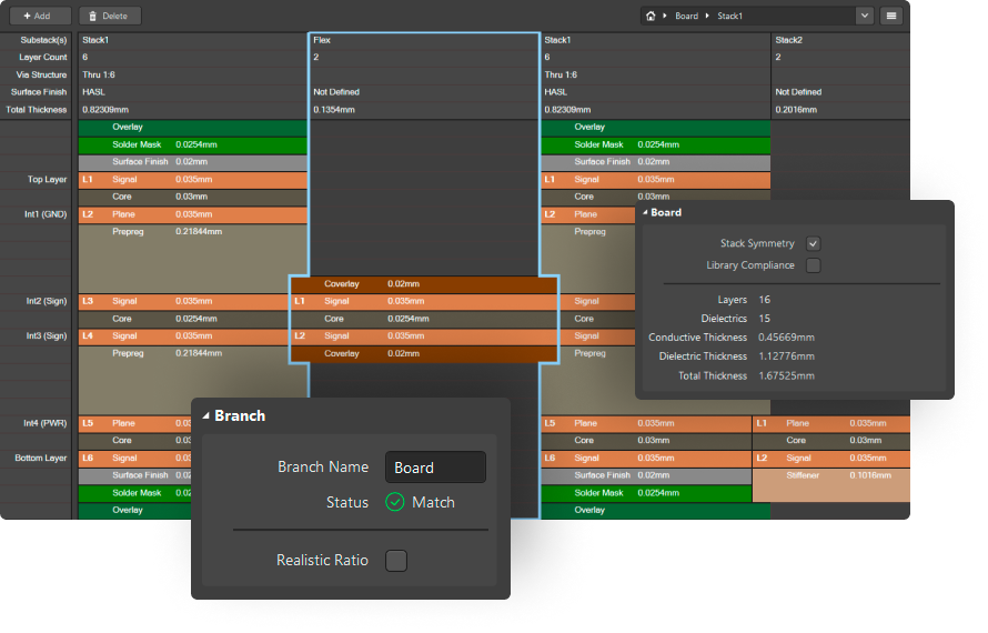
Altium Designer uses Top Overlay and Bottom Overlay as the primary silkscreen layers, corresponding to the physical top and bottom silkscreen prints. These mechanical layers stack with copper, solder mask, and paste in the layer stackup manager. Visibility toggles in the View Configuration panel allow isolation for editing, showing only overlay content against the board outline. Engineers set layer properties like color and transparency for optimal previewing during layout. Double-sided boards often mirror critical markings on both sides for accessibility.
Layer setup begins with confirming overlay activation in the PCB editor. Right-click layer tabs to enable Top Overlay, then select it as the active layer for placements. Design rules govern interactions, such as minimum clearances from copper features. This structured approach prevents common printing defects like ink bleed over exposed pads.
Altium Silkscreen Layer Setup
Altium silkscreen layer setup starts in the PCB editor by opening the View Configuration panel and enabling Top Overlay or Bottom Overlay visibility. Select the desired overlay as the active layer from the Layers list at the bottom of the screen. Access layer properties via the PCB Editor's Layer Configuration to adjust stack position if needed, though overlays remain non-copper mechanical layers. Define design rules under Design > Rules, creating a Clearance rule scoped to Silkscreen objects with targets like Pads or Vias, typically setting 4 to 6 mils minimum.
Next, configure Silkscreen-to-SolderMask Clearance rules to ensure ink does not encroach on mask openings. Use the online DRC to validate setup by running Design > Design Rule Check, selecting All Rules including Manufacturing clearances. This proactive verification catches violations early, maintaining design integrity. For multi-layer boards, repeat for both overlays, ensuring consistency across the stackup.
Engineers fine-tune via the Properties panel when placing primitives, locking layers to prevent accidental shifts. Export layer stacks to fabrication outputs confirms setup fidelity. Proper configuration supports automated silkscreen generation from schematics.
Creating Silkscreen Markings in Altium
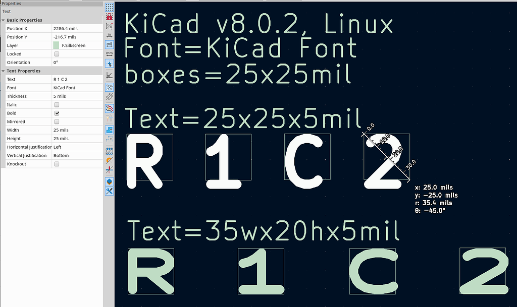
Creating silkscreen markings in Altium involves placing primitives directly on the overlay layer. Activate Top Overlay, then use Place > Text String for reference designators or labels, setting stroke width to 6 mils for legibility and height to 40 mils minimum. Draw component outlines with Place > Line or Arc, snapping to pad centers for alignment, especially pin-1 indicators on IC footprints. Polygons via Place > Polygon Pour fill irregular shapes like logos or borders, converting to regions for editing.
In the PCB Footprint Editor, define silkscreen per component for automatic population during update from schematic. Add outlines offset from pads per footprint standards, ensuring no overlap with solder joints. Back-annotate changes propagate ref des positions intelligently. Use the Properties panel to adjust justification, orientation, and font to TrueType or Stroke for vector scaling.
For batch edits, select multiple strings and edit globally. Verify with 3D view toggling silkscreen visibility. This method ensures markings survive netlist updates without manual rework.
IPC-7351 guidelines influence footprint silkscreen, specifying outline dimensions relative to land patterns for consistent component visualization.
Importing Logos into Altium Silkscreen
Importing logos into Altium silkscreen requires monochrome graphics for reliable printing. Prepare a BMP file in black and white using an image editor, saving as 1-bit monochrome. In the PCB editor, select Top Overlay, then Place > Graphic (or P, H shortcut), define the bounding rectangle, and choose the BMP file. The Import Image dialog previews the raster, allowing DPI adjustment and inversion if needed; set Composing to Union for a single editable object.
Paste method suits quick imports: copy monochrome BMP from Paint (Ctrl+A, Ctrl+C), switch to Altium overlay layer, and Ctrl+V to paste. Resize via right-click > Unions > Resize Union, dragging handles proportionally. SVG or PNG support vector scaling without pixelation, ideal for complex logos.
For OLE integration, insert BMP into Word, save, then Place > Object From File in Altium. Test print previews confirm fidelity. Avoid color images, as silkscreen inks are typically single-color white or matte black.
Position logos away from edges and high-heat zones to prevent peeling. This process integrates branding seamlessly into production files.
Best Practices and Silkscreen Preparation
Adhere to minimum line widths of 4 mils and character strokes of 6 mils to ensure printer resolution handles details without blurring. Space text at least 10 mils from pads and vias, using design rules to enforce globally. Orient markings parallel to board edges for readability, avoiding rotation beyond 90 degrees. Prioritize ref des near components, grouping passives logically to reduce clutter.
Employ the Silkscreen Preparation tool via Tools > Silkscreen Preparation for automated cleanup. Select All objects on overlay layers, enable Use Design Rules for clearance clipping, set Min Remaining Length to 5 mils, and activate Move Text with 20 mil Max Distance. Process fills by clipping to solder mask openings, delete externals beyond board shape, then review Messages panel for exceptions. Undo if needed, iterating for optimal results.
IPC-A-600K outlines acceptability criteria for markings, requiring legible identification without defects like pinholes or adhesion failures.
Separate regulatory symbols into dedicated footprint components with empty copper layers, placing as needed. Run DRC post-preparation to flag residuals.
IPC-SM-840E specifies performance tests for silkscreen adhesion and solvent resistance, guiding material selection indirectly through design robustness.
Troubleshooting Silkscreen Issues
Overlapping ref des from dense placement trigger DRC violations; resolve by editing positions in Interactive Move mode or using preparation clipping. Tiny text illegible post-print stems from insufficient stroke; scale up in Properties and recheck 1:1 zoom. Logos rasterizing poorly indicate non-monochrome source; reconvert to BMP and repaste.
Silkscreen on tented pads risks ink cracking during reflow; apply Silk to Solder Mask Expansion rule positively. Board outline intrusions get auto-removed in preparation, but verify mechanical layer alignment first. Schematic updates shifting ref des require targeted locks on custom text.
Persistent DRC ignores locked primitives; temporarily unlock, process, then relock. Isolate layers in gray scale mode for visual audits. These steps restore compliance efficiently.
Conclusion
Silkscreen design in Altium Designer demands precise layer setup, strategic marking placement, and rigorous preparation to deliver manufacturable boards. Key techniques like importing logos via monochrome BMP and leveraging the preparation tool minimize errors while enhancing usability. Adhering to clearances and legibility norms ensures assembly success and traceability. Electric engineers gain efficiency by integrating these practices early, from footprint creation to final outputs. Ultimately, robust silkscreen elevates PCB reliability across the product lifecycle.
FAQs
Q1: How do you perform Altium silkscreen layer setup?
A1: Altium silkscreen layer setup involves enabling Top Overlay or Bottom Overlay in the View Configuration panel and selecting it as active. Define clearance design rules for silk to pads and solder mask, typically 4-6 mils. Run DRC to verify, adjusting properties for stroke widths. This foundational step prevents printing defects and supports dual-sided markings. Proper setup integrates seamlessly with the layer stackup.
Q2: What are the steps for creating silkscreen markings in Altium?
A2: Creating silkscreen markings in Altium starts with activating the overlay layer and using Place > Text String for labels, Lines for outlines, and Polygons for shapes. Define in footprints for auto-placement, ensuring pin-1 indicators align with pads. Adjust via Properties for 6 mil stroke and 40 mil height. Use preparation tools to clip overlaps. This yields clear, error-free assemblies.
Q3: How to import logos into Altium silkscreen effectively?
A3: Importing logos into Altium silkscreen uses Place > Graphic for BMP/PNG/SVG files on overlay layers, previewing in the Import dialog with Union composing. Alternatively, paste monochrome BMP from Paint directly. Resize proportionally and position away from edges. Monochrome ensures reliable ink printing without artifacts. Verify in 3D and outputs for production readiness.
Q4: What best practices apply to silkscreen in Altium Designer?
A4: Best practices include 4 mil minimum lines, 10 mil clearances, and Silkscreen Preparation for clipping/moving conflicts. Place ref des near components, use stroke fonts, and isolate layers for review. Align with IPC standards for legibility. These ensure traceability and reduce fab rejects logically.
References
IPC-A-600K — Acceptability of Printed Boards. IPC, 2020
IPC-7351C — Generic Requirements for Surface Mount Design and Land Pattern Standard. IPC, 2014
IPC-SM-840E — Qualification and Performance Specification of Permanent Solder Mask. IPC, 2010


