Introduction
High Density Interconnect (HDI) PCBs represent a cornerstone of modern electronics, enabling unprecedented levels of integration in compact devices. As demands for smaller form factors grow in sectors like telecommunications, automotive, and medical equipment, HDI PCB technology trends continue to evolve rapidly. Engineers face the challenge of balancing signal integrity, thermal management, and reliability while pushing the boundaries of miniaturization trends. This article explores the next generation HDI PCB developments in miniaturization, advanced materials HDI innovations, and shifts in the future of PCB manufacturing. By examining these areas, electrical engineers can anticipate design choices that align with emerging industry capabilities. Understanding these trends ensures that future prototypes and production boards meet performance requirements without compromising manufacturability.
What Are HDI PCBs and Why Do They Matter?
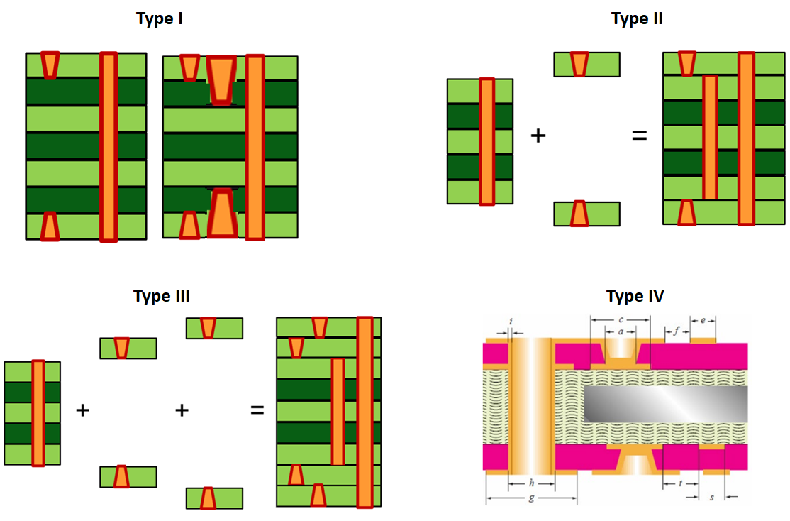
HDI PCBs differ from conventional boards through their use of finer lines, smaller vias, and higher layer counts to achieve greater wiring density per unit area, as defined in IPC-2226. These boards employ microvias, blind vias, and buried vias to connect layers efficiently, reducing overall board size while supporting complex routing. In an era of shrinking devices, HDI technology addresses the miniaturization trends driven by high-performance computing and 5G applications. For electrical engineers, HDI PCBs matter because they enable higher component densities, shorter signal paths for improved integrity, and support for fine-pitch components like BGAs with pitches below 0.4 mm. Without HDI advancements, achieving the interconnect density required for next generation HDI PCB designs would be impractical. This foundation sets the stage for ongoing innovations that directly impact design rules and fabrication feasibility.
Trends in Miniaturization for HDI PCBs
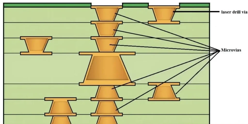
Miniaturization trends in HDI PCB technology trends focus on ultra-high density interconnects (UHDI), where line widths and spaces shrink to 40 microns or less, and microvia diameters approach 30 microns. Stacked and staggered microvia configurations allow for every-layer interconnects, maximizing routing efficiency in multilayer builds. Electrical engineers must consider via aspect ratios, typically limited to 1:1 or less, to ensure reliable plating and minimize drill smear. The shift toward any-layer vias eliminates traditional through-hole constraints, enabling true 3D routing architectures. These developments support the integration of more I/O in smaller footprints, critical for applications demanding high-speed data rates. As miniaturization advances, design tools must incorporate precise via-to-via spacing rules to prevent failures like cracking under thermal cycling.
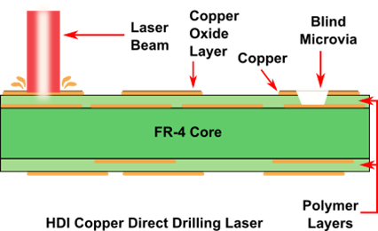
Sequential build-up (SBU) processes remain central, layering dielectrics and copper incrementally to form microvias with laser drilling. This method accommodates the thin cores needed for high layer counts, often exceeding 20 layers in compact boards. Engineers benefit from reduced parasitic inductance in signal paths, enhancing impedance control for frequencies above 10 GHz. However, challenges like warpage from mismatched CTEs intensify with thinner materials. Future designs will likely incorporate embedded traces within dielectrics for even finer features. These miniaturization trends redefine board real estate, allowing engineers to pack functionality previously requiring multiple boards into one.
Advanced Materials in HDI PCB Development
Advanced materials HDI selections prioritize low dielectric constant (Dk) and low dissipation factor (Df) for high-frequency performance, alongside high glass transition temperature (Tg) for reliability. Materials like modified epoxies and resin-coated copper (RCC) foil enable thin build-up layers under 50 microns, essential for tight via structures. Low-loss dielectrics reduce signal attenuation in mmWave applications, while high-Tg variants above 170°C withstand lead-free soldering profiles per J-STD-020. Electrical engineers evaluate CTE matching between copper and dielectric to prevent microvia breakout during reflow. Polyimide-based films offer flexibility for rigid-flex HDI hybrids, expanding applications in wearables. These material evolutions support the density increases without sacrificing electrical or mechanical integrity.
Build-up films with photoimageable dielectrics streamline via formation, allowing filled vias for surface mounting. Engineers must verify laser drill compatibility, as UV lasers excel with polymer dielectrics over CO2 types for ablating glass-filled resins. Thermal conductivity enhancements via ceramic fillers address hotspots in power-dense designs. Material stacks now include low-profile copper foils with reverse-treated surfaces for better adhesion in sequential lamination. As HDI complexity grows, hybrid material sets combining low-loss cores with high-reliability outer layers become standard. This strategic material use directly influences the future of PCB manufacturing by enabling finer features and robust yields.
Innovations in HDI PCB Manufacturing Processes
The future of PCB manufacturing for HDI boards hinges on precision processes like UV laser drilling, which achieves sub-50-micron vias with minimal heat-affected zones compared to mechanical methods. Plasma etching and desmear steps ensure clean via walls for electroless copper plating, critical for high-aspect blind vias. Electrical engineers appreciate direct imaging lithography for patterning traces below 30 microns, surpassing traditional photolithography limits. Embedded components, integrated during lamination, reduce assembly steps and improve reliability by minimizing solder joints. These techniques align with IPC-6012DS qualification requirements for HDI performance. Manufacturing shifts toward automation, including AI-driven inspection for defect detection in dense via fields.
Sequential lamination cycles build layers progressively, allowing staggered vias to share loads and enhance fatigue resistance. Engineers design with fan-out zones for microvias to inner layers, optimizing drill sequences. Solder mask advancements, like liquid photoimageable (LPI) with finer resolution, protect narrow traces from handling damage. Sustainability trends incorporate lead-free finishes and recyclable resins without compromising HDI capabilities. Yield improvements come from process controls like warp monitoring during pressing. These manufacturing evolutions enable scalable production of next generation HDI PCB designs.
Best Practices for Implementing HDI Trends
Electrical engineers should start with stackup simulations to predict impedance and crosstalk in miniaturized HDI layouts. Adhere to via fill requirements, using conductive or non-conductive pastes for planarity in via-in-pad designs. Thermal modeling identifies risks from current crowding in microvias, guiding trace width adjustments. Factory insights emphasize sequential verification after each build-up cycle to catch alignment drifts early. Collaborate on panel utilization to balance cost with density. These practices ensure designs transition smoothly to production.
Challenges like via reliability under shock testing demand robust plating thickness per IPC standards. Engineers mitigate warpage via symmetric stackups and constrained lamination. Signal integrity tools help route differential pairs with controlled lengths amid dense interconnects.
Conclusion
HDI PCB technology trends point to a future where miniaturization, advanced materials, and precise manufacturing converge for revolutionary electronics. Next generation HDI PCB capabilities will empower engineers to deliver compact, high-performance solutions reliably. By leveraging low-loss materials and laser-based processes, the industry addresses demands for speed and density. Staying aligned with standards ensures quality across the supply chain. Electrical engineers positioned to adopt these trends will drive innovation in their fields. The path forward promises even tighter integrations and enhanced functionalities.
FAQs
Q1: What are the key HDI PCB technology trends driving miniaturization trends today?
A1: HDI PCB technology trends emphasize ultra-fine lines under 40 microns, stacked microvias, and any-layer interconnects for higher density. Laser drilling enables smaller vias with better aspect ratios, supporting compact designs in high-speed applications. Engineers benefit from reduced board sizes while maintaining signal integrity. These shifts align with factory processes for reliable production. Future iterations will push UHDI limits further.
Q2: How do advanced materials HDI improve next generation HDI PCB performance?
A2: Advanced materials HDI like low Dk/Df dielectrics and high-Tg resins minimize losses and enhance thermal stability in dense boards. Thin build-up films support microvia formation without compromising adhesion. Electrical engineers select based on frequency needs and CTE matching for reliability. These materials enable finer features in sequential builds. Overall, they elevate speed and durability in modern electronics.
Q3: What role does laser drilling play in the future of PCB manufacturing for HDI?
A3: Laser drilling is pivotal in the future of PCB manufacturing, creating precise microvias for HDI density. UV lasers handle thin dielectrics with minimal taper, improving plating yields. It surpasses mechanical drilling for aspect ratios below 1:1. Engineers design around drill sequences for stacked configurations. This process supports embedded components and high-layer counts efficiently.
Q4: Why is IPC-2226 important for HDI PCB design guidelines?
A4: IPC-2226 provides essential design guidelines for HDI PCBs, defining wiring density and feature tolerances. It guides microvia placement, line spacing, and stackup rules for manufacturability. Electrical engineers use it to ensure compliance and reliability. The standard supports trends in miniaturization without fabrication risks. Adherence streamlines transitions from prototype to volume production.
References
IPC-2226 — Design Standard for High Density Interconnect (HDI). IPC.
IPC-6012DS — Qualification and Performance Specification for High Density Interconnect (HDI) Printed Boards. IPC.
J-STD-020E — Moisture/Reflow Sensitivity Classification for Nonhermetic Surface Mount Devices. JEDEC, 2014.


