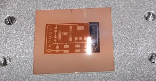
Introduction
High-speed PCB design demands meticulous attention to signal integrity amid rising data rates and shrinking rise times. Vias serve as critical interconnects in multilayer boards but introduce discontinuities through their plated barrels. The unused portion of these vias, known as stubs, extends beyond the target layers and acts as a source of impedance mismatch. Controlled depth drilling addresses this by precisely removing stubs, thereby minimizing reflections and preserving waveform fidelity. This technique proves essential for applications where signal quality directly influences system reliability. Engineers benefit from its integration to optimize performance without resorting to costlier alternatives like blind vias.
What Is Controlled Depth Drilling?
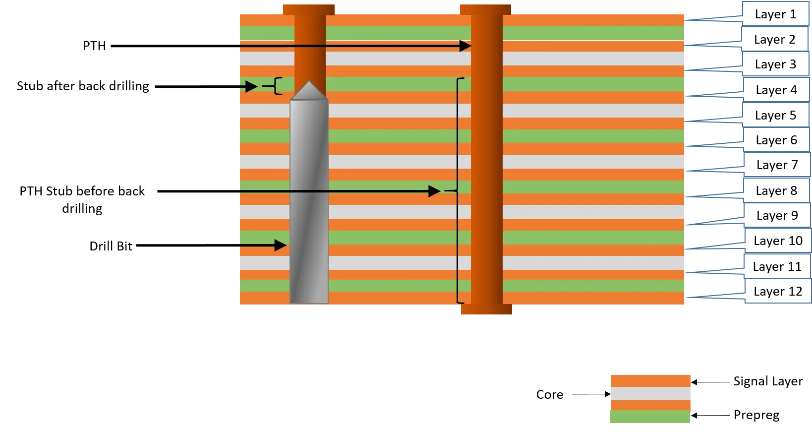
Controlled depth drilling, often termed backdrilling, represents a specialized manufacturing process applied after initial through-hole via formation. Standard through-vias are first drilled across the entire board thickness and electroplated to form conductive barrels. A secondary drilling step then employs a larger bit to excavate the stub from one or both sides, halting just above the innermost connected layer. This leaves a minimal remnant incapable of significantly affecting high-frequency signals. The process requires precise Z-axis control to avoid damaging functional copper.
Fabricators achieve depth accuracy through mechanical stops, optical sensing, or entry-exit board fixtures. Post-drilling, cleanup removes debris to prevent plating defects. This method suits rigid multilayer PCBs with layer counts exceeding eight.
Why Controlled Depth Drilling Matters for High-Speed PCB Design
In high-speed environments, signals behave as guided waves sensitive to trace and via geometries. Long via stubs create parallel transmission paths that branch off the main signal route. At frequencies where stub length approaches a quarter wavelength, they resonate and reflect energy back toward the source. Such reflections superimpose on incoming signals, causing distortion, increased bit error rates, and compliance failures.
Without mitigation, these effects limit routing lengths and layer usage in dense designs. Controlled depth drilling extends viable interconnect distances by rendering stubs electrically short. It supports higher data rates while maintaining eye diagram margins. For electrical engineers tackling gigabit interfaces, this technique unlocks greater design flexibility.
Technical Principles of Via Stubs and Their Impact on Signal Integrity
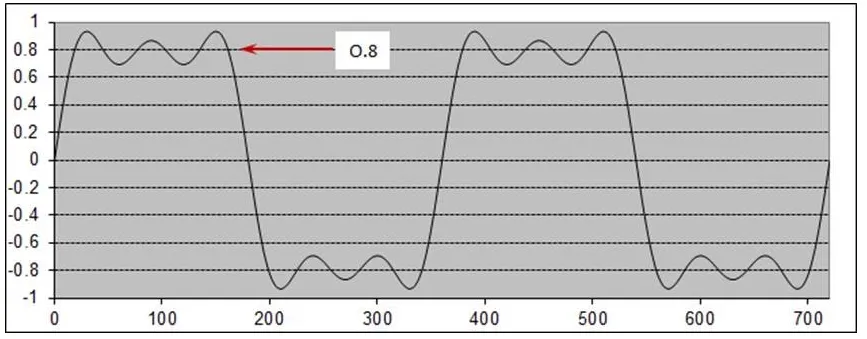
Via stubs function as reactive elements with both inductive and capacitive components. The open end of the stub produces a reflection coefficient near unity for signals in its passband. This leads to periodic nulls in frequency response and ringing in time domain. Engineers observe these via time-domain reflectometry, where stubs manifest as low-impedance dips after the via plateau.
Impedance matching falters because the stub alters the effective characteristic impedance along the propagation path. Signal integrity suffers from accumulated phase shifts and amplitude variations. Controlled depth drilling shortens stubs below critical thresholds relative to signal rise times. Consequently, reflections diminish, and the via approximates an ideal feedthrough.
The mechanism aligns with transmission line theory, where stub effects scale inversely with frequency. High-speed PCB design thus prioritizes stub minimization for broadband performance.
Key Controlled Depth Drilling Benefits in Reducing Signal Reflections
Controlled depth drilling benefits center on eliminating stub-induced parasitics. Shorter stubs reduce return loss, allowing more signal power to reach the receiver. This translates to improved insertion loss profiles across wide bandwidths. Differential signaling pairs gain from symmetric stub removal, preserving balance and common-mode rejection.
Reducing signal reflections enhances overall signal integrity by minimizing deterministic jitter components. Eye patterns exhibit cleaner openings with reduced closure risks. Impedance matching becomes more predictable, easing compliance with protocol specifications. Electromagnetic interference also drops as fewer stub resonances radiate energy.
Designers achieve higher routing densities without via optimization trade-offs. These advantages prove invaluable in backplanes and server boards.
Best Practices for Controlled Depth Drilling in High-Speed PCB Design
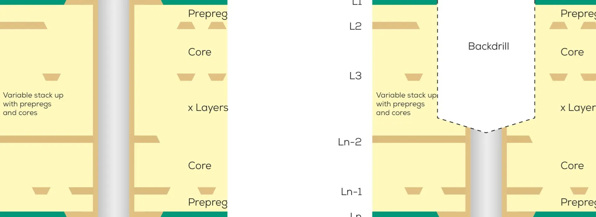
Start with stackup planning to pair signal layers appropriately for single-side backdrilling where possible. Specify depths from outer layers, incorporating material tolerances for accuracy. Provide generous clearance between backdrill edges and inner traces to prevent breakthrough. IPC-6012 outlines requirements for plated-through hole features and depth control in multilayer boards.
In design files, denote backdrill targets with net-specific callouts and oversize drill charts. Simulate via stubs using 3D electromagnetic tools to validate lengths against frequency goals. Select backdrill diameters typically larger than vias for complete copper removal without residue.
Fabrication notes should detail verification methods like coupon sections. Post-process inspection via cross-sectioning confirms acceptability per IPC-A-600 criteria. Limit application to critical high-speed nets to balance cost and benefit. IPC-2221 offers guidance on managing via discontinuities in design phases.
Collaborate early with manufacturers on capability matrices for depth tolerances.
Challenges and Troubleshooting in Implementation
Depth variations arise from board warpage, drill wander, or inconsistent entry points. Asymmetric stackups complicate dual-side access. Overdrilling risks exposing inner layers, while underdrilling leaves functional stubs. Engineers troubleshoot via simulation sweeps and prototype TDR measurements.
Material selection influences drillability; harder cores demand robust tooling. Verify fabricator processes align with class 3 requirements for high-reliability apps. Iterative design refinements based on fab feedback refine outcomes.
Conclusion
Controlled depth drilling transforms high-speed PCB performance by systematically addressing via stub limitations. It fortifies signal integrity, refines impedance matching, and curbs reflections through precise manufacturing. Electrical engineers gain a reliable tool for multilayer interconnects in demanding systems. Adhering to established standards ensures consistent results across production runs. Embracing this technique elevates design margins and accelerates time-to-market.
FAQs
Q1: What are the primary controlled depth drilling benefits for high-speed PCB design?
A1: Controlled depth drilling removes via stubs that cause impedance discontinuities and reflections, preserving signal integrity for fast-edged signals. It improves return and insertion loss without resorting to complex blind-via structures, enhancing design efficiency in multilayer boards and supporting higher data rates with lower jitter.
Q2: How does controlled depth drilling improve signal integrity and reduce reflections?
A2: By excavating unused via stubs, backdrilling eliminates resonant paths that reflect energy at high frequencies. The shortened remnants have negligible electrical length relative to signal wavelengths, producing smoother impedance profiles and cleaner waveforms, with reduced insertion loss and crosstalk in high-speed designs.
Q3: When is controlled depth drilling essential for impedance matching?
A3: Use it on through-vias in thick stackups where stub length exceeds acceptable thresholds for target frequencies, especially on nets susceptible to reflection-induced jitter. Combine with precise trace impedance control to achieve robust matching for high-speed interfaces.
Q4: How do industry standards guide controlled depth drilling practices?
A4: Standards such as IPC-6012 define fabrication tolerances for depth-controlled holes and plating integrity, while IPC-A-600 provides inspection criteria for stub remnants. These references help ensure reliability and consistency in high-speed applications, balancing performance with manufacturability.
References
IPC-6012E — Qualification and Performance Specification for Rigid Printed Boards. IPC, 2017
IPC-A-600K — Acceptability of Printed Boards. IPC, 2020
IPC-2221B — Generic Standard on Printed Board Design. IPC, 2012