Introduction
High-power PCB design demands robust solutions for handling elevated currents and heat loads, where thick copper layers play a pivotal role in enhancing current-carrying capacity and thermal management in high-power PCBs. Sequential lamination emerges as a critical manufacturing process for building complex multilayer structures, particularly in HDI PCB power distribution systems that require blind and buried vias. However, the integration of heavier copper weights introduces unique challenges during multiple lamination cycles, affecting board flatness, via reliability, and overall yield. Engineers must understand these interactions to optimize performance without compromising manufacturability. This article explores the technical implications of copper weight variations in sequential lamination, drawing from established manufacturing principles to guide high-power PCB design decisions.
Understanding Sequential Lamination and Copper Weight in High-Power Applications
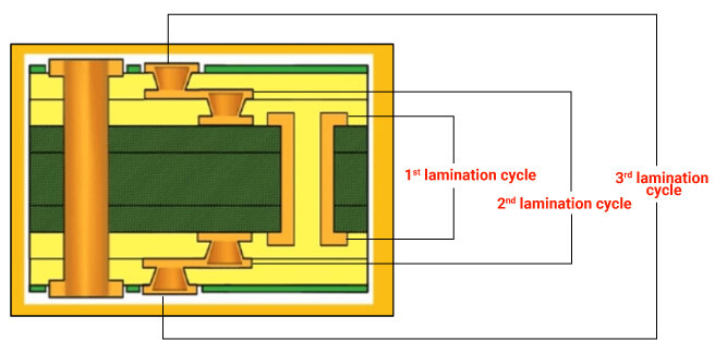
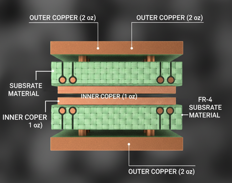
Sequential lamination involves fabricating PCBs through successive bonding cycles, starting with cores or sub-stacks of copper-clad laminates and prepregs, followed by imaging, drilling, plating, and additional laminations. This method enables high-density interconnects essential for compact high-power designs, allowing stacked or staggered vias that reduce signal path lengths. Copper weight, typically measured in ounces per square foot, dictates the foil thickness, with standard 1 oz equating to about 35 microns and thick copper exceeding 2 oz for power planes.
In high-power PCBs, thicker copper improves HDI PCB power distribution by minimizing voltage drops and I2R losses across wide traces. Yet, sequential lamination copper weight directly influences process control, as heavier foils demand precise resin flow to fill gaps between layers adequately. Factory insights reveal that unbalanced copper distribution across layers exacerbates issues like incomplete filling or voids, underscoring the need for symmetric stackups in production.
Technical Mechanisms: How Copper Weight Influences Lamination Dynamics
Thicker copper foils alter the coefficient of thermal expansion (CTE) mismatch between metal and dielectric materials during lamination under heat and pressure. As copper expands differently from the resin system, residual stresses build up, potentially leading to warpage that propagates through sequential cycles. This effect intensifies with heavier weights on inner layers, where subsequent outer laminations struggle to maintain planarity for accurate drilling and registration.
Resin requirements scale with copper thickness; for instance, areas retaining more copper post-etching necessitate additional prepreg to achieve uniform dielectric thickness. Inadequate flow results in starved regions or delamination risks, particularly in high-aspect-ratio vias formed during buildup. Per IPC-6012 guidelines for rigid board qualification, controlled lamination parameters mitigate these risks, ensuring minimum copper wrap plating thickness and void-free bonds.
Drilling challenges escalate with thick copper PCB constructions, as mechanical drills face higher breakthrough forces and smear on heavy inner layers, complicating desmear processes before plating. Laser drilling for blind vias in sequential steps also encounters reflectivity issues with thicker foils, impacting ablation efficiency. These mechanisms collectively demand adjusted process windows, including higher pressures or specialized fillers, to preserve interlayer alignment.
Key Challenges in Thick Copper Sequential Lamination
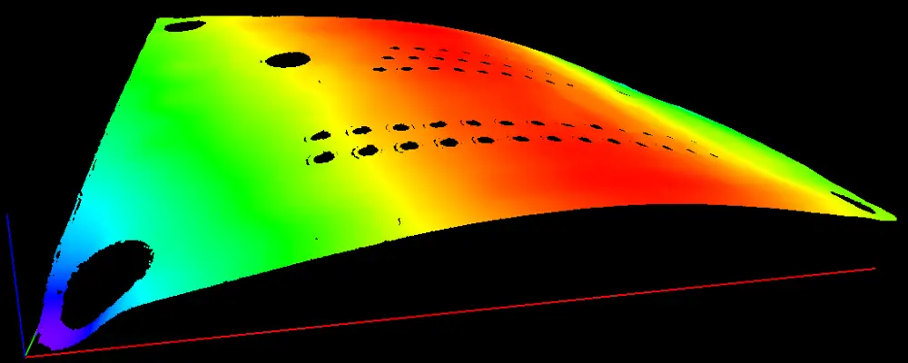
Warpage stands out as a primary concern, driven by asymmetric copper weight across the stackup, which induces bowing during cool-down after lamination. Factory-driven observations confirm that panels exceeding certain copper asymmetries fail flatness specs, rendering them unusable for high-precision HDI features. Thermal gradients during multiple cycles amplify this, as thicker power planes retain heat longer, causing differential contraction.
Via reliability suffers in thick copper environments, with plated-through holes prone to cracking under thermal cycling due to increased stress at copper-dielectric interfaces. Sequential lamination copper weight variations can lead to inconsistent plating thickness, violating minimum wrap requirements and risking electromigration in high-power applications. Etching tolerances tighten for heavy foils, as undercuts widen, necessitating wider line widths that inflate board size.
Thermal management in high-power PCBs intersects here, where thick copper aids heat spreading but complicates dissipation paths if warpage distorts via barrels. Overly rigid stacks from heavy copper reduce flexibility, heightening bow-and-twist beyond acceptable limits post-lamination.
Best Practices for Mitigating Copper Weight Effects
Designers should prioritize symmetric copper distribution, mirroring weights on opposing layers to balance CTE stresses throughout sequential lamination. Stackup planning tools help visualize resin budgets, ensuring sufficient prepreg plies for flow around thick foils without excess squeeze-out. High-Tg materials, selected per IPC-4101 laminate specs, enhance flow control and resist deformation under repeated press cycles.
Process adjustments include plasma cleaning for better adhesion and optimized drill parameters to handle thick copper breakthrough. For HDI PCB power distribution, hybrid constructions blending standard and heavy copper layers minimize sequential steps while maximizing current paths. IPC-2226 provides HDI design guidelines, emphasizing via aspect ratios under 1:1 for reliable plating in buildup processes.
In thermal management in high-power PCBs, integrate embedded thermal vias early, plated to match power plane weights for uniform heat transfer. Factory validation through bow-and-twist measurements post each lamination cycle ensures compliance before proceeding.
Integrating Thermal Management with Sequential Lamination
Thick copper excels in lateral heat spreading, crucial for high-power modules where components generate localized hotspots. Sequential lamination allows precise placement of power and ground planes adjacent to heat sources, but copper weight must align with via fill strategies to avoid thermal bottlenecks. Plugged or filled vias enhance vertical conduction, complementing heavy planes.
Challenges arise when heavy copper impedes uniform heating during lamination, leading to hot spots that cure resin unevenly. Best practices involve ramped pressure profiles and carrier plates to distribute force evenly. This synergy ensures robust HDI PCB power distribution without thermal runaway risks.
Conclusion
Copper weight profoundly shapes sequential lamination outcomes in high-power PCB design, balancing enhanced electrical and thermal performance against manufacturability hurdles like warpage and via integrity. By adhering to symmetric designs, material selections, and process controls aligned with IPC standards, engineers can harness thick copper benefits effectively. Factory insights emphasize proactive stackup optimization to sustain yield in complex builds. Ultimately, informed decisions on sequential lamination copper weight elevate reliability in demanding applications.
FAQs
Q1: What role does copper weight play in warpage during sequential lamination?
A1: In sequential lamination, heavier copper weights create CTE mismatches with dielectrics, generating stresses that cause warpage, especially in asymmetric stackups. Balanced distribution across layers minimizes bowing, ensuring flatness for subsequent drilling and plating in high-power PCB design. Factories monitor this via post-lamination bow-and-twist tests to maintain process control.
Q2: How does thick copper affect HDI PCB power distribution in sequential builds?
A2: Thick copper enhances current capacity and reduces impedance in power planes, vital for HDI PCB power distribution. However, it requires adjusted resin flow and drilling in sequential lamination to prevent voids or misalignment. Symmetric designs per IPC guidelines optimize performance while preserving via reliability.
Q3: Why is thermal management critical with sequential lamination copper weight?
A3: Thermal management in high-power PCBs relies on thick copper for heat spreading, but sequential lamination amplifies risks like uneven curing from retained heat in heavy foils. Using high-Tg materials and thermal vias ensures efficient dissipation, preventing hotspots that degrade long-term reliability.
Q4: What best practices address challenges in thick copper sequential lamination?
A4: Prioritize symmetric copper weights, precise resin budgeting, and plasma desmear for adhesion in sequential lamination copper weight processes. Adhering to IPC-6012 for qualification verifies plating integrity, supporting robust high-power PCB design without yield losses.
References
- IPC-6012E - Qualification and Performance Specification for Rigid Printed Boards. IPC, 2015
- IPC-2226G - Design Standard for High Density Interconnect (HDI). IPC, 2019
- IPC-4101F - Specification for Base Materials for Rigid and Multilayer Printed Boards. IPC, 2016


