Introduction
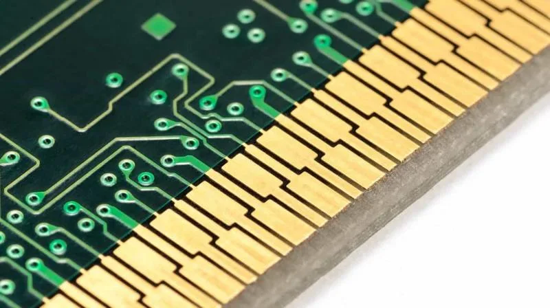
Gold fingers serve as critical edge connectors in printed circuit boards, enabling reliable electrical interfaces in applications ranging from memory modules to graphics cards. These gold-plated contacts demand pristine surfaces for optimal mating with sockets, where even minor imperfections can compromise performance. Solder mask, the protective polymer layer applied over the PCB copper traces, plays a dual role by insulating circuits while potentially interfering with gold finger functionality if not managed properly. Issues like solder mask encroachment on gold fingers or inadequate solder mask clearance for gold fingers can lead to contact failures, increased insertion forces, and degraded signal transmission. This article explores these interactions, focusing on engineering principles and practical strategies to maintain high reliability. Electric engineers must prioritize precise design and fabrication controls to ensure gold fingers perform under repeated mating cycles.
Understanding Gold Fingers and Solder Mask in PCBs
Gold fingers consist of elongated copper pads electroplated with nickel and a thin layer of hard gold to provide corrosion resistance and low contact resistance. They are typically beveled at the insertion edge to facilitate smooth socket engagement and are positioned along the PCB periphery for modular connectivity. Solder mask, often liquid photoimageable (LPI) material, is screen-printed or photolithographically applied to cover non-contact areas, preventing oxidation, short circuits, and environmental degradation. In gold finger regions, the solder mask must be completely opened to expose the full contact surface, as any residue can act as an insulator or contaminant. During PCB fabrication, the solder mask layer is defined in Gerber files with precise openings aligned to the gold finger pads. Proper delineation ensures the mask terminates cleanly beyond the finger boundaries, adhering to standards like IPC-6012E for rigid board performance.
The interaction between solder mask and gold fingers begins in the design phase, where engineers specify mask openings that extend beyond the pad edges. Fabrication tolerances for mask alignment typically require verification to avoid overlap. Encroachment occurs when mask material flows or misaligns during curing, partially covering the gold surface. This phenomenon heightens risks in high-density boards where thermal expansion during processing exacerbates edge effects. Engineers evaluate these factors through design rule checks (DRC) in CAD software, ensuring compatibility with manufacturing capabilities.
Solder Mask Clearance for Gold Fingers: Design Essentials
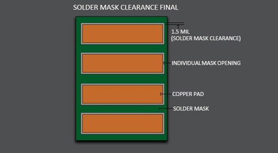
Solder mask clearance for gold fingers refers to the minimum distance between the mask edge and the gold-plated contact boundary, critical for preventing contamination and ensuring beveling processes. Inadequate clearance can lead to mask peeling during edge milling or gold plating inconsistencies, as the mask acts as a barrier for plating solutions. Engineers design clearances to accommodate fabrication tolerances, typically specifying openings that fully encompass the finger length and width plus a buffer zone. This buffer allows for photoresist development variations and solder mask expansion under UV exposure and baking. During electrical testing, proper clearance maintains low contact resistance by avoiding insulating layers at the mating interface. Visual inspection post-fabrication confirms clearance integrity, with automated optical inspection (AOI) tools detecting anomalies.
Clearance requirements intensify for beveled gold fingers, where mechanical routing removes material after mask application, potentially dislodging nearby mask if too close. Standards such as IPC-A-600K outline acceptability criteria for mask coverage, emphasizing no protrusion onto exposed conductors. Engineers balance clearance with board density, as excessive openings may expose adjacent traces to solder wicking during assembly. Finite element analysis can model thermal stresses on mask edges near fingers, predicting potential encroachment. Consistent clearance application across production runs minimizes yield losses from rework.
Solder Mask Encroachment on Gold Fingers: Causes and Consequences
Solder mask encroachment on gold fingers happens when the mask material advances beyond its intended boundary, often due to overexposure, underdevelopment, or flow during thermal cure. This creates thin films or blobs on the gold surface, increasing insertion and extraction forces while reducing wipe contact effectiveness. Contaminated fingers exhibit higher mating resistance, leading to fretting corrosion over cycles as micro-movements abrade the mask-gold interface. In high-reliability applications, such defects accelerate wear, shortening connector lifespan. Engineers detect encroachment via cross-section microscopy, revealing mask thickness variations along the finger bevel.
Fabrication factors like panel warpage contribute to misalignment, where differential shrinkage pulls mask toward edges. High-viscosity mask inks resist flow better but demand precise application control. Encroachment disrupts gold plating uniformity, as mask overhangs shield underlying copper, causing voids or thin spots. Signal paths connected to encroached fingers suffer intermittent connectivity, evident in continuity tests. Mitigation starts with Gerber file verification, ensuring mask layers align with copper pads within tolerances defined by IPC-6012E.
Effects of Solder Mask on Signal Integrity
The effects of solder mask on signal integrity near gold fingers stem from changes in local dielectric properties and mechanical stability. While gold fingers themselves carry signals, proximal mask influences impedance continuity from traces to contacts. Thick or uneven mask alters the effective dielectric constant, introducing reflections in high-speed interfaces operating above 1 GHz. Encroachment exacerbates this by creating capacitive coupling irregularities at the finger base. Engineers model these effects using field solvers to predict return loss and crosstalk.
Mask material's loss tangent affects attenuation, particularly if residue contaminates the gold surface, promoting oxidation beneath. In differential signaling, asymmetric mask coverage skews pair impedance, degrading eye diagrams. Thermal cycling induces mask cracking near fingers, introducing intermittent paths that couple noise. Compliance with IPC-A-600K ensures mask adhesion prevents delamination, preserving baseline integrity. Simulations incorporating mask thickness variations guide design iterations for robust performance.
Solder Mask Materials for Gold Fingers
Solder mask materials for gold fingers must exhibit low outgassing, high adhesion to nickel underplating, and resistance to plating chemistries. LPI masks dominate due to fine-line resolution, enabling precise openings around dense finger arrays. Epoxy-based formulations provide mechanical robustness, while acrylate variants offer faster curing for high-volume production. Compatibility ensures no bleeding during gold immersion or electrolytic plating, which could deposit mask particles on contacts. Engineers select masks with CTE matching the substrate to minimize stress at finger edges.
Material selection influences long-term reliability, as hydrolysis-prone masks degrade in humid environments, leading to blistering near gold areas. UV-curable masks reduce solvent emissions but require post-bake for hardness. Testing per IPC-TM-650 methods verifies mask integrity post-plating. Hybrid materials blending flexibility and rigidity suit flex-rigid boards with gold fingers. Overall, material choice aligns with application demands, prioritizing clean exposure for fingers.
Preventing Solder Bridging on Gold Fingers
Preventing solder bridging on gold fingers involves shielding contacts during wave or selective soldering of nearby components. Gold fingers must remain solder-free to avoid embrittlement from tin-gold intermetallics, which increase contact resistance. Full solder mask openings over fingers eliminate bridging sites, while temporary masks protect during flux application. Design separates fingers from solder-wettable areas by at least standard trace spacing. Assembly processes employ fixtures to mask edges, preventing flux entrapment.
Bridging risks rise with dense pin fields adjacent to fingers, where capillary action draws molten solder. Engineers specify non-wetting gold finishes and verify via X-ray post-assembly. Mask dams between traces reinforce prevention without encroaching on fingers. IPC J-STD-001 guidelines for assemblies stress clean contact zones. Proactive fab notes request edge connector protection, ensuring zero solder on gold surfaces.
Best Practices for Optimizing Gold Finger Performance
Implement solder mask clearance for gold fingers by specifying 0.1 mm minimum buffers in design files, verified through DFM reviews. Use AOI and flying probe testing to inspect for encroachment post-mask application. Opt for beveling after plating to avoid mask damage, with full-area exposure during mask processing. Simulate thermal profiles to predict mask flow, adjusting cure parameters accordingly. Standardize on high-resolution LPI masks for tight tolerances. Incorporate fiducials near finger arrays for alignment precision. Conduct accelerated life testing per IPC-TM-650 to validate mating cycles under load. Collaborate with fabricators on panelization to minimize warpage-induced shifts. Document all layers with exploded views for clarity. These practices ensure gold fingers meet performance specs reliably.
Conclusion
Solder mask profoundly influences PCB gold finger performance through clearance, encroachment risks, signal integrity effects, material choices, and bridging prevention. Engineers achieve excellence by integrating precise design rules, rigorous inspection, and standards-compliant processes. Adhering to IPC-6012E and IPC-A-600K guarantees quality from fab to assembly. Proactive management yields durable connectors for demanding applications. Prioritizing these best practices enhances overall PCB reliability and longevity.
FAQs
Q1: What is the recommended solder mask clearance for gold fingers?
A1: Solder mask clearance for gold fingers ensures clean exposure and prevents contamination during plating and beveling. Engineers specify openings extending beyond pad edges to accommodate tolerances, typically verified via Gerber checks and AOI. This maintains low contact resistance and facilitates socket mating. Proper clearance aligns with IPC-A-600K acceptability criteria for exposed conductors.
Q2: How does solder mask encroachment on gold fingers affect performance?
A2: Solder mask encroachment on gold fingers introduces insulating layers, raising insertion forces and promoting fretting wear. It disrupts plating uniformity, leading to higher resistance and potential signal dropouts. Detection via microscopy guides rework, while design buffers mitigate risks. Consistent fab controls per IPC-6012E prevent recurrence.
Q3: What are the effects of solder mask on signal integrity for gold fingers?
A3: The effects of solder mask on signal integrity arise from dielectric variations and contamination near fingers. Uneven coverage alters impedance, causing reflections in high-speed paths. Modeling with field solvers optimizes layouts. Mask-free fingers preserve trace-to-contact continuity effectively.
Q4: How to prevent solder bridging on gold fingers during assembly?
A4: Preventing solder bridging on gold fingers requires full mask openings and edge protection fixtures. Non-wettable gold repels solder, while spacing from assembly zones avoids capillary action. Post-process inspection confirms cleanliness, ensuring reliable connectivity.
References
IPC-6012E — Qualification and Performance Specification for Rigid Printed Boards. IPC, 2015
IPC-A-600K — Acceptability of Printed Boards. IPC, 2020
IPC-2221B — Generic Standard on Printed Board Design. IPC, 2003


