Introduction
In high-power PCB design, managing heat dissipation is critical to ensuring performance and longevity of electronic systems. As power densities increase in modern applications, components generate significant thermal energy, which can degrade reliability if not addressed. Thermal vias serve as a vital solution, providing a pathway for heat to transfer from hot components to heat sinks or ground planes. This article explores the role of thermal vias, focusing on thermal via design guidelines, placement strategies, diameter considerations, copper plating techniques, and the importance of thermal simulation. Aimed at electrical engineers, this discussion offers practical insights into optimizing PCB layouts for thermal management. By understanding these principles, designers can enhance system reliability and prevent failures in demanding environments.
What Are Thermal Vias and Why Do They Matter
Thermal vias are small conductive pathways drilled through a printed circuit board to facilitate heat transfer between layers. Typically filled or plated with copper, they connect heat-generating components on the surface to internal or bottom layers, often linked to ground planes or heat sinks. Their primary function is to reduce thermal resistance, allowing heat to dissipate efficiently. In high-power applications, such as power supplies, LED lighting, and automotive electronics, excessive heat can cause component failure, reduced lifespan, and signal integrity issues. Thermal vias mitigate these risks by creating low-resistance paths for heat flow. Without proper thermal management, localized hot spots can develop, leading to thermal stress and potential system breakdowns. Thus, incorporating thermal vias is essential for maintaining operational stability in high-power PCB designs.
Technical Principles of Thermal Vias in Heat Dissipation
The effectiveness of thermal vias relies on fundamental principles of heat transfer, primarily conduction. Heat generated by components flows through the via's copper plating to cooler areas of the PCB, such as ground planes or external heat sinks. The thermal conductivity of copper, combined with the via's structure, determines how efficiently this transfer occurs. Several factors influence performance, including via diameter, copper plating thickness, and the number of vias used. Larger diameters and thicker plating reduce thermal resistance, enhancing heat flow. Additionally, vias placed directly under or near heat sources maximize their impact. However, designers must balance these factors with electrical considerations, as excessive vias can interfere with signal routing or increase parasitic capacitance. Understanding these principles is key to optimizing thermal via design guidelines for specific applications.
Thermal Via Design Guidelines for Optimal Performance
Designing thermal vias requires adherence to established practices to ensure effective heat dissipation while maintaining PCB integrity. Below are key guidelines for engineers working on high-power designs.
- Material Selection: Use copper for via plating due to its high thermal conductivity. Ensure consistent plating thickness to avoid weak spots that hinder heat transfer.
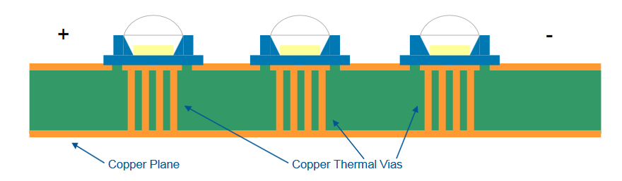
- Via Count and Spacing: Place multiple vias under or around heat-generating components. Spacing should be uniform to prevent thermal bottlenecks, typically following a grid pattern.
- Connection to Planes: Connect thermal vias to large copper planes, such as ground or power planes, to spread heat across a wider area. Avoid isolating vias from these planes.
- Avoid Overcrowding: While increasing via count improves heat dissipation, excessive vias can compromise structural integrity or disrupt signal traces. Balance is critical.
These guidelines align with industry standards, such as IPC-6012E, which specifies performance criteria for vias in rigid PCBs. Following such standards ensures reliability in high-power applications.
Suggested Reading: Mastering Thermal Vias: Essential Heat Management for High-Power PCBs
Thermal Via Placement Strategies for Maximum Efficiency
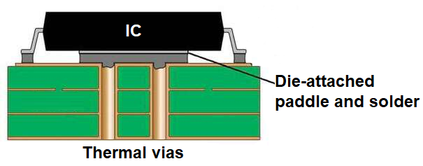
Thermal via placement plays a crucial role in managing heat dissipation. Positioning vias directly beneath or adjacent to heat-generating components, such as power transistors or ICs, minimizes the distance heat must travel. This reduces thermal resistance and prevents hot spots. When possible, connect vias to the largest available copper plane on inner or bottom layers to distribute heat evenly. For components with thermal pads, such as QFN packages, place vias within the pad area to maximize contact. Additionally, consider the PCB's overall layout to avoid placing vias near sensitive signal traces, as they can introduce noise. Effective thermal via placement requires careful planning during the design phase to align with both thermal and electrical requirements of the system.
Determining Thermal Via Diameter for Heat Transfer
The diameter of thermal vias directly impacts their ability to conduct heat. Larger diameters provide lower thermal resistance, allowing more heat to pass through. However, practical constraints, such as available board space and drilling capabilities, often limit via size. Common diameters range between 0.3 mm and 0.6 mm for standard PCBs, balancing heat transfer with manufacturability. Smaller vias may be used in dense layouts, but their effectiveness decreases due to reduced cross-sectional area. When selecting a diameter, engineers must also consider the aspect ratio, or the ratio of via depth to diameter, to ensure proper copper plating. Standards like IPC-A-600K provide guidance on acceptable via dimensions and tolerances, ensuring designs meet reliability criteria for high-power applications.
Importance of Thermal Via Copper Plating Quality
Copper plating within thermal vias is critical for effective heat conduction. The plating thickness and uniformity determine how well heat transfers through the via. Thin or uneven plating increases thermal resistance, reducing performance. Industry standards, such as IPC-6012E, specify minimum plating thicknesses for vias to ensure consistent quality. Typically, a plating thickness of 20 to 25 micrometers is recommended for thermal vias in high-power designs. Additionally, filled vias, where the hole is completely filled with copper, offer superior thermal conductivity compared to hollow plated-through holes. However, filled vias are costlier and may not be necessary for all applications. Engineers must evaluate the thermal demands of their design to choose the appropriate copper plating method for optimal results.
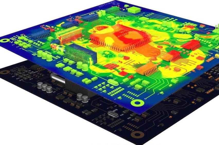
Leveraging Thermal Simulation for Design Validation
Thermal simulation is an indispensable tool for validating thermal via designs before manufacturing. By modeling heat flow within a fast turn PCB, engineers can predict temperature distributions, identify hot spots, and assess the effectiveness of thermal vias. Simulation software allows for testing various configurations, such as different via counts, diameters, and placements, without building physical prototypes. Key inputs for accurate simulation include material properties, power dissipation values, and boundary conditions like ambient temperature. Outputs typically show temperature gradients and thermal resistance, guiding design adjustments. Using thermal simulation early in the design process helps optimize layouts for heat dissipation, reducing the risk of costly redesigns. This approach aligns with best practices for ensuring reliability in high-power PCB applications.
Practical Challenges and Solutions in Thermal Via Implementation
Implementing thermal vias in high-power PCB designs presents several challenges. One common issue is balancing thermal performance with electrical constraints. Excessive vias under components can interfere with signal integrity by introducing parasitic effects. To address this, limit via placement to areas away from high-speed traces or use shielding techniques. Another challenge is manufacturing variability, such as inconsistent copper plating, which can degrade thermal performance. Adhering to standards like IPC-A-600K for via quality inspection helps mitigate this risk. Additionally, thermal vias may increase production costs, especially with filled vias. Engineers can optimize costs by prioritizing vias only in critical areas. By anticipating these challenges and applying targeted solutions, designers can achieve effective thermal management without compromising other design aspects.
Conclusion
Thermal vias are a cornerstone of effective heat dissipation in high-power PCB design. By providing low-resistance pathways for heat transfer, they prevent component overheating and enhance system reliability. Success depends on following thermal via design guidelines, optimizing thermal via placement, selecting appropriate thermal via diameter, ensuring high-quality thermal via copper plating, and utilizing thermal simulation for validation. These practices, grounded in industry standards like IPC-6012E and IPC-A-600K, enable engineers to address thermal challenges in demanding applications. As power densities continue to rise, mastering thermal via implementation becomes increasingly vital for creating robust and efficient electronic systems. Thoughtful design and rigorous analysis are essential to achieving optimal performance.
FAQs
Q1: How does thermal via placement affect heat dissipation in high-power PCBs?
A1: Thermal via placement is critical for efficient heat dissipation. Positioning vias directly under or near heat-generating components minimizes thermal resistance, allowing heat to transfer quickly to copper planes or heat sinks. Poor placement can lead to hot spots, reducing reliability. Engineers must balance placement with signal routing to avoid interference while maximizing thermal performance.
Q2: What factors determine the ideal thermal via diameter for a PCB design?
A2: The ideal thermal via diameter depends on heat transfer needs, board space, and manufacturing constraints. Larger diameters reduce thermal resistance, improving heat flow, but space limitations often restrict size. Common diameters range from 0.3 to 0.6 mm. Standards like IPC-A-600K provide guidance on acceptable dimensions to ensure manufacturability and performance.
Q3: Why is thermal via copper plating quality important for PCB reliability?
A3: Thermal via copper plating quality directly impacts heat conduction. Uniform, thick plating ensures low thermal resistance, enhancing heat transfer. Thin or uneven plating can create bottlenecks, leading to overheating. Following standards like IPC-6012E for minimum plating thickness is essential to maintain reliability in high-power PCB designs under thermal stress.
Q4: How can thermal simulation improve thermal via design guidelines?
A4: Thermal simulation predicts temperature distribution and identifies hot spots before manufacturing. It allows testing of various thermal via configurations, such as count and placement, to optimize heat dissipation. By simulating real-world conditions, engineers can refine designs, reduce risks, and ensure compliance with thermal performance goals in high-power applications.
References
IPC-6012E — Qualification and Performance Specification for Rigid Printed Boards. IPC, 2020.
IPC-A-600K — Acceptability of Printed Boards. IPC, 2020.


