Introduction
Just-in-time (JIT) PCB production has transformed how electronics manufacturers operate by minimizing inventory costs and enabling rapid response to market demands. In this model, printed circuit boards move quickly from design to fabrication and assembly without excess stockpiling, which puts immense pressure on design accuracy. Design for manufacturing (DFM), or design for manufacturability PCB practices, plays a pivotal role here by ensuring that PCB layouts are optimized for seamless production flows. Poor DFM can lead to defects, rework, or delays that undermine JIT efficiency, while strong DFM for JIT PCB strategies boost first-pass yields and shorten lead times. Electrical engineers must integrate DFM early to align designs with factory capabilities, avoiding common pitfalls in high-speed production environments. This article explores how DFM PCB best practices enable reliable JIT PCB production.
Understanding Design for Manufacturability in PCBs
Design for manufacturability PCB refers to the systematic approach of creating PCB layouts that are easy to fabricate, assemble, and test while meeting performance requirements. It involves anticipating manufacturing constraints like material properties, tooling limits, and process variations from the initial design stage. In the context of JIT production, DFM becomes essential because there is little margin for error or multiple prototyping runs. Engineers apply DFM guidelines to select standard features that reduce setup times on production lines, such as conventional drill sizes and routing paths. By following these principles, designs achieve higher manufacturability, directly supporting the lean principles of JIT where production matches demand precisely. Ultimately, DFM bridges the gap between engineering intent and factory reality.
Why DFM Matters in Just-in-Time PCB Production
JIT PCB production thrives on short lead times, often measured in days rather than weeks, making any design flaw costly in terms of delayed shipments. Traditional batch production tolerates some redesigns, but JIT demands near-perfect designs to avoid bottlenecks in etching, drilling, or lamination processes. DFM for JIT PCB minimizes these risks by incorporating factory-driven insights that prevent issues like insufficient annular rings or asymmetric stackups leading to warpage. High first-pass yields from manufacturable PCB designs reduce scrap and overtime labor, preserving the cost advantages of JIT. Electrical engineers benefit from DFM by gaining predictable outcomes, allowing focus on innovation rather than firefighting production problems. In essence, DFM ensures JIT remains agile and responsive.
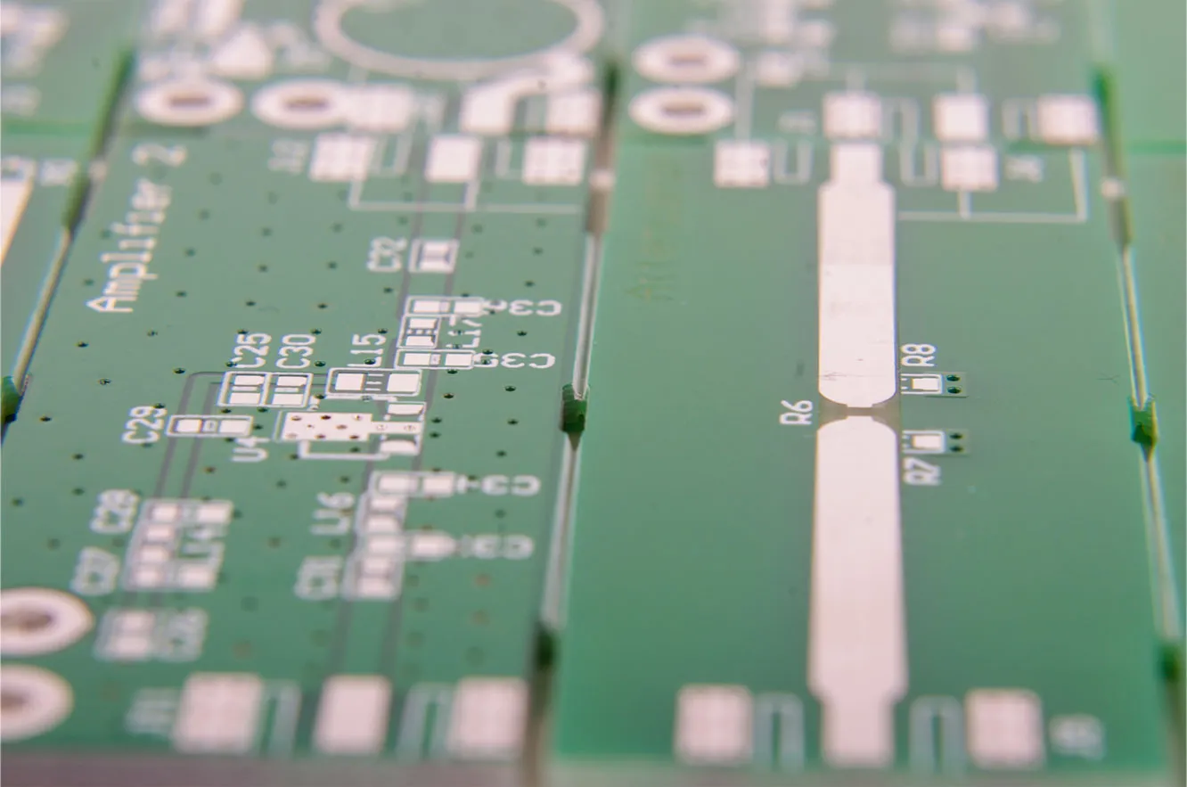
Key Technical Principles of DFM for JIT PCBs
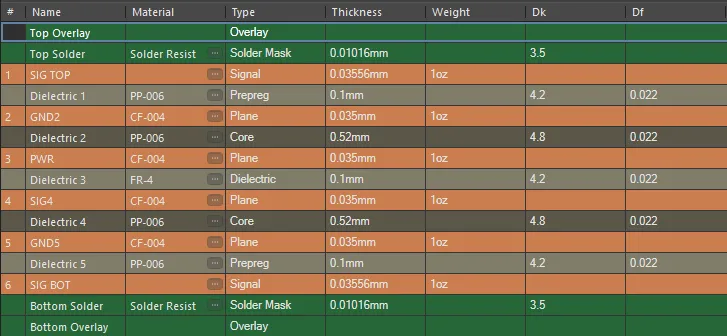
Effective DFM starts with symmetric layer stackups to control warpage, a critical factor in multilayer boards processed under JIT timelines. Uneven copper distribution causes bow and twist during lamination or reflow, potentially exceeding acceptable limits and halting assembly lines. IPC-6012F outlines performance specifications that guide maximum allowable warpage for rigid boards, emphasizing balanced constructions. Engineers should distribute copper planes evenly across layers and use core materials with matched coefficients of thermal expansion. This principle not only meets standards but also speeds up qualification in fast-paced JIT environments. Proper stackup planning thus forms the foundation of robust DFM PCB guidelines.
Another core principle involves conductor spacing and widths that align with fabrication tolerances. Traces too narrow or closely spaced risk opens or shorts during etching, especially in high-volume JIT runs where consistency is paramount. Adhering to IPC-2221C generic design standards ensures minimum clearances that accommodate process variations without compromising signal integrity. For vias and pads, maintaining adequate annular rings prevents drill breakout, a frequent cause of rejects. These choices reduce inspection times and enable automated optical checks common in JIT factories. Overall, these mechanisms enhance yield while supporting dense, high-performance layouts.
Panelization techniques represent a vital DFM aspect for JIT scalability. Individual boards arrayed on standard panels optimize material use and streamline depanelization, cutting handling steps. V-scoring suits rectangular boards for clean, high-speed separation, while tab-routing handles irregular shapes with mouse bites for tool-free singulation. Both methods require fiducial marks for precise alignment during exposure and placement. Poor panel design leads to uneven stress distribution and warpage in JIT batches. By prioritizing these principles, engineers enable efficient throughput from panel to finished product.
DFM PCB Best Practices for Optimal JIT Production
Start with standard board dimensions and outlines to leverage existing tooling in JIT facilities, avoiding custom setups that extend lead times. Rectangular shapes with rounded corners facilitate routing and prevent stress concentrations during depanelization. Incorporate breakaway tabs or rails on panels for stable fixturing in automated lines. These practices align with manufacturable PCB design by reducing changeover durations between jobs. Engineers can further enhance flow by specifying standard hole sizes and aspect ratios that match common drill inventories. Consistent application yields faster quoting and fabrication starts.
Fiducials and tooling holes are non-negotiable for alignment in high-precision JIT processes. Place global fiducials in opposite corners of panels, at least 0.1 inch from edges, with local ones near fine-pitch components. These laser-etched marks ensure sub-micron accuracy for imaging and pick-and-place, minimizing offsets that plague assembly. Clear solder mask openings around fiducials prevent registration errors. Integrating these early in DFM checks supports seamless transitions to assembly. Factories appreciate such foresight, as it cuts programming time for vision systems.
Copper balance extends beyond stackups to plane splits and fill patterns. Asymmetric fills induce thermal gradients during pressing, exacerbating warpage beyond IPC-A-600M acceptability criteria. Use ground pours judiciously, mirroring patterns on opposing layers where possible. For high-current paths, follow current-carrying capacity guidelines to avoid overheating in reflow. These best practices prevent field failures while accelerating JIT validation. Electrical engineers gain reliability without sacrificing density.
Solder mask and silkscreen application demands precise clearances to avoid bridging or bleed. Define mask expansion around pads per class requirements, ensuring exposure for wetting without encroachment on traces. Legend placement should avoid vias and high-heat zones to maintain legibility post-assembly. In JIT, these details prevent cosmetic rejects that slow shipping. Combining with via tenting strategies enhances protection in humid environments. DFM PCB best practices like these foster defect-free boards at speed.
Routing and scoring paths influence mechanical integrity in depanelized boards. Maintain minimum distances from outlines to components, allowing router clearance without damage. V-grooves require straight lines parallel to edges, with optimal angles for stress relief. Tab-routing needs uniform bite sizes for consistent separation force. These guidelines reduce microcracks, especially in rigid-flex hybrids. JIT production benefits from such forethought through lower warranty claims.
Common Challenges and Troubleshooting in DFM for JIT
Warpage remains a top challenge in JIT due to rapid thermal cycling in lamination. Asymmetric builds or mismatched materials amplify this, often detected late in inspection. Troubleshoot by simulating stackups for CTE balance and verifying against IPC specifications. Factory insights recommend thinner cores for better control in high-layer counts. Addressing early via DFM reviews prevents batch-wide scrapping.
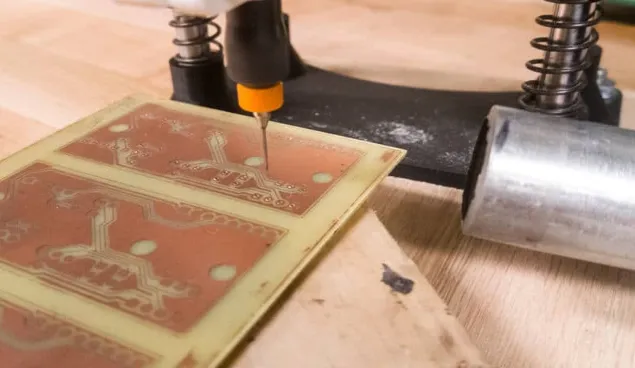
Drill smear and breakout plague high-aspect holes in dense designs. JIT lines favor mechanical drilling, so limit ratios to standard capabilities. Post-plating inspections per IPC-A-600M catch issues before assembly. Engineers can mitigate with teardrop pads and larger annular rings. Proactive DFM turns potential delays into strengths.
Component keepouts near edges or scores risk damage during handling. Define mechanical zones excluding tall parts or connectors under insertion stress. This practice safeguards JIT flows from mechanical failures. Troubleshooting involves iterative DFM checklists aligned with factory feedback.
Conclusion
Design for manufacturing profoundly shapes the success of just-in-time PCB production by embedding manufacturability into every layout decision. From symmetric stackups and standard panelization to precise fiducials and clearances, DFM PCB guidelines ensure high yields and minimal delays. Electrical engineers adopting these practices align designs with factory realities, maximizing JIT benefits like cost savings and agility. Prioritizing DFM for JIT PCB not only meets standards like IPC-2221C but elevates overall product quality. As production demands intensify, mastering manufacturable PCB design remains a competitive edge.
FAQs
Q1: What is DFM for JIT PCB and why is it essential?
A1: DFM for JIT PCB involves optimizing designs for rapid, error-free fabrication in just-in-time environments. It focuses on features like standard sizes and balanced copper to achieve high first-pass yields. Without it, defects cause delays, inflating costs in low-inventory models. Electrical engineers use DFM to streamline from Gerber to shipment, ensuring reliability under tight schedules.
Q2: What are key DFM PCB best practices for panelization?
A2: Key DFM PCB best practices include using V-scoring for straight-edged boards and tab-routing for complex shapes, always with fiducials for alignment. Maintain copper symmetry to control warpage and add rails for handling stability. These reduce depanelization risks and speed JIT throughput. Follow standards for clearances to avoid stress cracks.
Q3: How does design for manufacturability PCB prevent warpage in JIT production?
A3: Design for manufacturability PCB prevents warpage through symmetric stackups and even copper distribution, adhering to IPC-6012F limits like 0.75% maximum bow and twist. Balance layers and select matched materials to counter thermal stresses. In JIT, this avoids assembly rejects and rework. Simulate early to validate.
Q4: What role do IPC standards play in DFM PCB guidelines?
A4: IPC standards like IPC-2221C and IPC-A-600M provide DFM PCB guidelines for spacing, annular rings, and acceptability. They ensure designs suit factory processes in JIT settings. Referencing them minimizes variations and boosts yields. Engineers apply them for consistent, manufacturable outcomes.
References
IPC-2221C - Generic Standard on Printed Board Design. IPC, 2023
IPC-6012F - Qualification and Performance Specification for Rigid Printed Boards. IPC, 2023
IPC-A-600M - Acceptability of Printed Boards. IPC, 2025