Introduction
In the evolving landscape of modular electronics, board-to-board connections play a crucial role in enabling compact, scalable systems. PCB edge plating emerges as a key technology for these connections, providing robust electrical and mechanical interfaces without relying on bulky discrete connectors. This approach supports high-density designs where space constraints demand efficient mating surfaces. Electrical engineers often encounter challenges in ensuring reliable signal transmission and structural integrity during repeated insertions. PCB edge plating addresses these needs by metallizing board edges, facilitating direct contact in stacked or adjacent configurations. As systems grow more complex, understanding this process becomes essential for optimizing performance.
What Is PCB Edge Plating and Why It Matters for Board-to-Board Connections
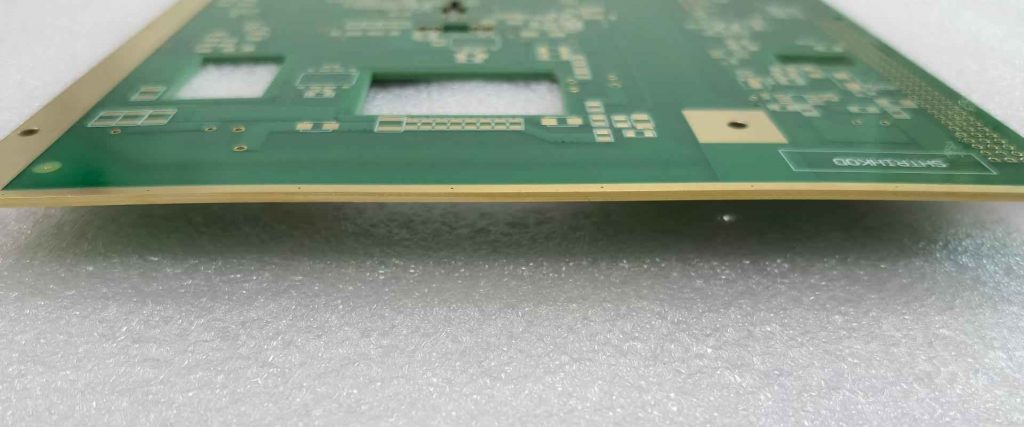
PCB edge plating involves depositing conductive metal layers, typically copper with nickel and gold finishes, along the perimeter or specific sections of a printed circuit board edge. This creates continuous conductive paths from inner layers to the board surface, ideal for PCB edge connectors in board-to-board setups. Unlike traditional connectors, edge plating uses the board itself as the mating interface, reducing assembly height and cost in modular electronics. It comes in forms like full perimeter plating for shielding, selective gold fingers for signal contacts, or castellated edges for module docking. Compliance with IPC-2221A ensures proper design for these edge-board connectors, emphasizing material selection and geometry.
The significance lies in its contribution to reliability under mechanical stress and environmental exposure. In board-to-board applications, unplated edges risk poor contact, signal degradation, or delamination at layer interfaces. Edge plating prevents crack propagation between layers, enhances grounding, and improves EMI shielding, critical for high-speed signals. For modular electronics, it enables hot-swappable modules and stacked assemblies common in servers, telecom gear, and embedded systems. Engineers benefit from fewer failure points, as plated edges withstand insertion cycles better than bare copper. This technology aligns with demands for miniaturization while maintaining performance standards.
Technical Principles of PCB Edge Plating in Board-to-Board Connections
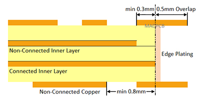
The plating process begins with electroless copper deposition to seed non-conductive surfaces, followed by electrolytic copper buildup for thickness and conductivity. Nickel acts as a barrier layer to prevent diffusion, topped with gold for corrosion resistance and low contact resistance in PCB edge connectors. This stack ensures the edge maintains electrical continuity from top to bottom layers, vital for board-to-board signal paths. During fabrication, edges are routed post-plating or masked selectively to avoid plating in non-contact areas. Beveling or chamfering the leading edge reduces wear during mating, as outlined in design guidelines for edge-board connectors.
In board-to-board contexts, edge plating forms male contacts that mate with female sockets or adjacent plated edges. The plating bridges ground planes, minimizing impedance discontinuities and crosstalk at high frequencies. Mechanical strength increases as the metal sheath reinforces the laminate against flexing or warping. For modular electronics, castellated plating—semicircular pads along the edge—allows precise alignment and soldering to carrier boards. Signal integrity improves due to shorter paths and shielding, reducing loop inductance. IPC-6012E specifies performance qualifications for such rigid boards, including edge integrity under thermal cycling.
Cross-sectional uniformity is key; variations in plating thickness can lead to hot spots or intermittent contacts. Plating chemistry controls throwing power to cover vertical edges evenly, despite gravity effects in vertical racks. Post-plating inspection verifies adhesion and voids, ensuring compliance before assembly. In stacked configurations, multiple boards leverage shared plating for common grounds, simplifying routing. This principle extends to RF applications where edge plating contains fields, preventing radiation.
Practical Solutions and Best Practices for PCB Edge Plating Assembly
Design starts with defining edge zones free of components, typically 3 mm clearance, to accommodate plating and mating tolerances. Route traces to edge pads with adequate annular rings for plating wrap-around, avoiding thin sections prone to voids. Specify plating extent in fabrication notes, distinguishing signal fingers from ground bars. For PCB edge plating board-to-board, align pad pitch with socket requirements and incorporate keying notches for polarization. Simulate insertion forces to validate bevel angles and plating hardness.
During manufacturing, apply solder mask to protect non-plated areas, ensuring no encroachment on contact surfaces. Post-routing plating uses specialized fixtures to handle edges, achieving uniform coverage. Cleanliness prevents contamination that could cause dewetting or oxidation. Qualification per IPC-6012E involves cross-section analysis for layer continuity and adhesion pull tests.
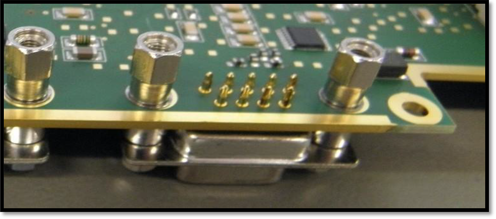
In PCB edge plating assembly, J-STD-001 guides soldering of castellated edges to host boards, emphasizing flux selection and preheat to avoid tombstoning. Use low-insertion-force sockets for gold fingers to preserve plating life. Automated optical inspection verifies contact flatness post-mating. For modular electronics, standardize edge profiles across modules for interchangeability. Thermal profiling during reflow accounts for plating's heat dissipation effects.
Troubleshooting common issues requires systematic checks. Poor adhesion often stems from inadequate surface activation; remedy with plasma cleaning. Voids in plating indicate gas entrapment—adjust bath agitation. Intermittent contacts trace to uneven gold thickness; measure with XRF and replate if below spec. Delamination at edges signals moisture ingress; bake boards pre-assembly. Warpage exacerbates misalignment—counter with symmetric layer stacks. Visual cues like discoloration flag oxidation; inspect under magnification early.
Troubleshooting Insights for Reliable Board-to-Board Performance
Engineers frequently debug failures in PCB edge plating board-to-board connections, starting with continuity tests across layers. Use flying probe for edge traces before mating. Microsection suspect edges to reveal plating defects like dog-boning or skips. For signal issues, TDR analysis pinpoints impedance bumps at edges.
Mechanical failures from repeated cycles demand cycle testing per application life. Gold wear exposes nickel, increasing resistance—monitor with four-point probes. In humid environments, creep corrosion attacks platings; specify hard gold alloys. Vibration-induced fretting responds to increased normal force via socket design.
Case insights from high-reliability sectors show selective plating reduces costs while targeting critical paths. Hybrid approaches combine edge plating with press-fit pins for power. Data logging during qualification correlates defects to process parameters, refining yields.
Conclusion
PCB edge plating stands as a cornerstone for robust board-to-board connections in modular electronics, balancing electrical performance with mechanical durability. From design per IPC-2221A to assembly under J-STD-001, adherence to standards ensures repeatability. Engineers gain flexibility in dense layouts, with shielding and grounding benefits enhancing overall system integrity. Troubleshooting empowers proactive fixes, extending field life. As demands for scalability rise, this technology will underpin next-generation interconnects.
FAQs
Q1: What are the main benefits of PCB edge plating for board-to-board connections?
A1: PCB edge plating board-to-board enhances signal integrity by providing low-impedance paths and shielding, while boosting mechanical strength against insertions. It eliminates discrete connectors, saving space in modular electronics. Ground continuity across layers reduces EMI, and corrosion-resistant finishes ensure long-term reliability. Practical assembly simplifies with direct mating, though design must account for tolerances.
Q2: How does PCB edge plating assembly differ from standard processes?
A2: PCB edge plating assembly requires selective masking and post-routing plating to cover vertical surfaces uniformly. J-STD-001 criteria apply for soldering castellated edges, focusing on flux coverage and void-free joints. Inspection emphasizes edge flatness and plating adhesion. Troubleshooting targets voids via bath chemistry tweaks, differing from planar surface finishes.
Q3: When should electrical engineers specify PCB edge connectors with plating?
A3: Opt for PCB edge connectors in space-constrained modular electronics needing frequent mating or high-speed signals. Plating is essential for grounding and shielding in RF stacks. Avoid in low-cycle, cost-sensitive apps where sockets suffice. Assess via cycle life and impedance needs during design review.
Q4: What common issues arise in PCB edge plating for modular electronics?
A4: Voids, adhesion loss, and uneven thickness plague edges due to poor throwing power. Warpage misaligns contacts during board-to-board mating. Oxidation from handling degrades gold fingers. Mitigate with process controls, beveling, and IPC-6012E qualification for consistent performance.
References
IPC-2221A — Generic Standard on Printed Board Design. IPC.
IPC-6012E — Qualification and Performance Specification for Rigid Printed Boards. IPC, 2017.
IPC J-STD-001 — Requirements for Soldered Electrical and Electronic Assemblies. IPC.


