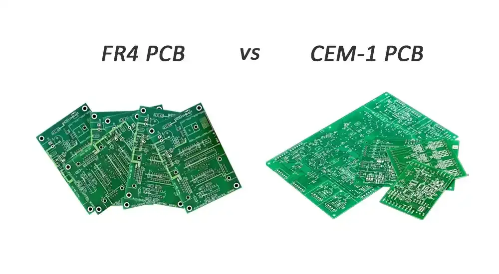
Introduction
Internet of Things (IoT) devices have transformed industries by enabling connectivity and data-driven decisions across smart homes, industrial automation, and healthcare systems. At the heart of every IoT device lies the printed circuit board (PCB), serving as the foundational platform for integrating sensors, microcontrollers, and communication modules. PCB manufacturers play a pivotal role in IoT hardware development, bridging the gap between conceptual designs and reliable, production-ready boards. Their expertise ensures that PCBs meet the stringent demands of compact size, low power consumption, and robust wireless performance. Without skilled manufacturing partners, IoT projects risk delays, failures, or suboptimal performance in real-world deployments. This article explores how PCB manufacturers contribute to successful IoT device development through design collaboration, process optimization, and adherence to quality standards.
Why PCB Manufacturers Matter in IoT Device Development
IoT devices demand PCBs that support high-density interconnects and mixed-signal environments, where analog sensors coexist with digital processors and RF components. Manufacturers provide the technical know-how to translate iot pcb requirements into manufacturable layouts, anticipating challenges like signal integrity and thermal management early in the process. They offer design for manufacturability (DFM) feedback, which prevents costly iterations by identifying issues such as inadequate clearances or via reliability under vibration. In fast-paced IoT projects, this partnership accelerates time-to-market while maintaining functionality in diverse environments, from battery-powered wearables to edge computing nodes. Engineers benefit from manufacturers' experience with evolving materials that balance cost, performance, and environmental resilience. Ultimately, selecting a capable PCB manufacturer elevates iot hardware from prototype to scalable production.
Key Challenges in Designing PCBs for IoT Devices
IoT applications impose unique constraints on PCB design for iot, including miniaturization to fit small form factors and support for multiple wireless protocols like Wi-Fi, Bluetooth, and Zigbee. High-frequency signals in wireless pcb design require controlled impedance traces and minimal crosstalk, which standard FR-4 materials may not fully support without enhancements. Power efficiency is critical, as devices often run on limited batteries, necessitating careful layer stackups to minimize resistive losses and enable efficient power planes. Environmental factors, such as humidity and temperature cycling, further complicate reliability, demanding boards with low coefficient of thermal expansion mismatches. Manufacturers address these by recommending high-Tg laminates and precise plating thicknesses during the quoting phase. Overcoming these hurdles ensures iot pcb longevity and compliance with operational specs.
The Manufacturer's Role in PCB Design for IoT
PCB manufacturers collaborate closely with engineers on pcb design for iot, providing stackup simulations and material recommendations tailored to wireless performance. They analyze schematics for routing feasibility, suggesting adjustments like blind vias for HDI boards common in compact IoT modules. In wireless pcb design, factories emphasize symmetry in ground planes and via fencing to suppress EMI, drawing from production data on yield rates. This input refines designs before fabrication, reducing scrap and respins. Manufacturers also facilitate prototyping with quick-turn services, allowing iterative testing of antenna tuning and signal paths. Their factory-driven insights ensure designs align with high-volume capabilities, such as panel utilization for cost efficiency.
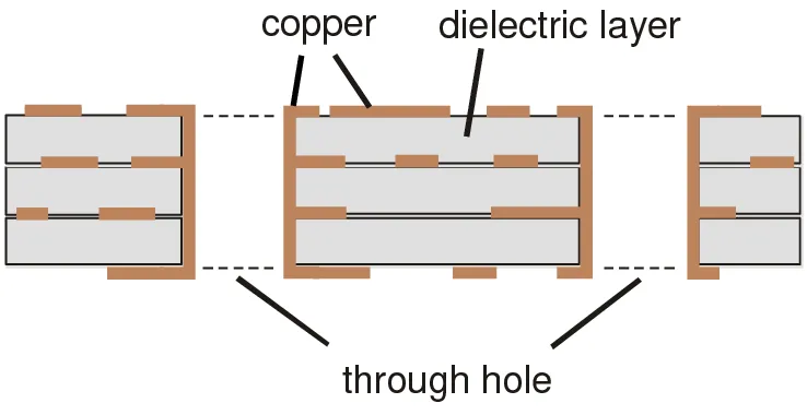
Manufacturing Processes Optimized for IoT Hardware
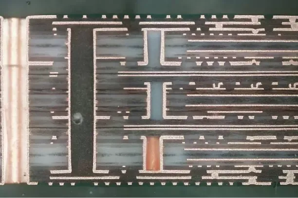
Fabricating iot pcb involves advanced processes like laser direct imaging for fine-line features under 3/3 mil geometries, essential for dense sensor integrations. Multilayer builds, often 8-12 layers, incorporate embedded passives and cavities for shielding sensitive RF sections in iot hardware. Controlled depth drilling and filled vias enhance thermal dissipation, critical for processors handling edge AI workloads. Solder mask and silkscreen applications provide conformal coatings for moisture resistance in outdoor IoT deployments. Sequential lamination enables complex wireless pcb design with mixed dielectrics for optimal RF propagation. These processes, refined through years of production, deliver boards ready for automated assembly.
Wireless PCB Design: Manufacturing Considerations
Wireless pcb design demands precise control of dielectric constants and loss tangents to maintain signal integrity up to 5 GHz or higher. Manufacturers specify Rogers or similar low-loss cores for high-performance layers while using cost-effective hybrids for base layers. Trace width calculators and field solver feedback during design review prevent deviations that cause insertion loss. Antenna integration requires clear keep-out zones and matching networks fabricated with tight tolerances on via capacitance. Factories test for return loss post-fabrication, offering coupons for customer verification. This meticulous approach ensures reliable connectivity in crowded spectrum environments typical of IoT ecosystems.
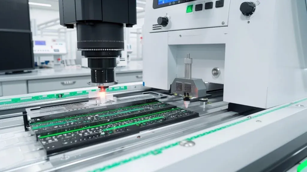
Quality Control and Standards in IoT PCB Production
Quality assurance in pcb for iot devices starts with incoming material inspections and extends through automated optical inspection (AOI) and X-ray for hidden defects. IPC-A-600K criteria guide visual acceptability, ensuring no voids or delaminations that could fail under thermal stress. Traceability via barcode systems tracks each panel from drill to final test, vital for field failure analysis in deployed IoT networks. Electrical testing verifies netlist integrity and shorts, while flying probe adapts to low-volume prototypes. Adherence to ISO 9001:2015 frameworks standardizes these procedures across operations. Robust quality control minimizes downtime in connected IoT systems.
Best Practices for Collaborating with PCB Manufacturers on IoT Projects
Engineers should share Gerber files with drill and fab drawings early, incorporating DFM checklists for via fill and solder dam specs. Specify IPC-6012E class 3 requirements for high-reliability iot pcb in mission-critical applications. Request stackup drawings with copper weights and prepreg schedules to align on thermal performance. Conduct joint design reviews focusing on wireless pcb design hotspots like baluns and filters. Prototype with enhanced IPC Class 3 to de-risk production ramps. These practices foster seamless transitions from design to manufacturing, optimizing yield and performance.
Emerging Trends in PCB Manufacturing for IoT
As IoT scales, manufacturers adopt flexible and rigid-flex PCBs for wearable and curved devices, combining polyimide substrates with fine-pitch components. Integration of 5G modules pushes for higher layer counts and microvias, with factories investing in plasma etching for cleaner surfaces. Sustainability drives lead-free processes and recyclable materials without compromising RF properties. Edge computing demands larger boards with more copper for power delivery networks. Manufacturers evolve capabilities to support these shifts, ensuring iot hardware remains competitive. Forward-thinking partnerships position teams for next-generation deployments.
Conclusion
PCB manufacturers are indispensable in IoT device development, transforming complex requirements into reliable iot pcb that power connected ecosystems. Their expertise in pcb design for iot, wireless pcb design, and production processes ensures signal integrity, power efficiency, and durability. By leveraging standards-aligned quality control and proactive collaboration, engineers achieve faster prototyping and scalable manufacturing. As IoT expands, partnering with proficient manufacturers will drive innovation in iot hardware. Prioritizing these relationships unlocks the full potential of interconnected technologies.
FAQs
Q1: What makes PCB for IoT devices different from standard PCBs?
A1: PCBs for IoT devices prioritize miniaturization, low-power routing, and RF optimization to support wireless connectivity and sensors in compact forms. Manufacturers focus on HDI structures and low-loss materials to handle mixed signals without interference. This differs from standard PCBs by emphasizing impedance control and thermal vias for battery life. Collaboration ensures manufacturability from the start.
Q2: How do PCB manufacturers support wireless PCB design?
A2: Manufacturers provide stackup expertise and impedance modeling for traces carrying Wi-Fi or Bluetooth signals in iot pcb. They recommend dielectric layering to minimize losses and suggest ground plane strategies for EMI suppression. Design reviews catch routing issues early, improving yield. Post-fab testing verifies performance margins. This support is crucial for reliable wireless pcb design in dense environments.
Q3: Why is quality control essential in IoT hardware PCB production?
A3: Quality control in IoT hardware prevents field failures from defects like microcracks or plating voids, which amplify under vibration or cycling. Standards like IPC classes ensure traceability and electrical reliability for always-on devices. Automated inspections catch issues invisible to the eye, boosting confidence in deployments. Manufacturers' rigorous processes safeguard network integrity.
Q4: What role does DFM play in PCB design for IoT?
A4: DFM in pcb design for iot identifies fabrication limits like minimum annular ring or aspect ratios before production. Manufacturers flag potential yield killers, such as dense via fields in wireless sections. Adjustments enhance panel efficiency and reduce costs. This iterative feedback shortens development cycles for iot pcb projects.
References
IPC-A-600K — Acceptability of Printed Boards. IPC, 2020
IPC-6012E — Qualification and Performance Specification for Rigid Printed Boards. IPC, 2017
ISO 9001:2015 — Quality Management Systems. ISO, 2015