Introduction
In high-density interconnect (HDI) printed circuit boards, microvias serve as critical interconnects to achieve denser routing and smaller form factors. PCB microvia filling addresses challenges associated with unfilled or partially filled vias, such as planarity issues and reliability under thermal stress. This guide explores materials, methods, and reliability considerations for effective PCB microvia filling. Engineers designing multilayer HDI boards must understand these aspects to ensure performance in demanding applications like smartphones, automotive electronics, and medical devices. By filling microvias, manufacturers create robust structures that support stacked vias and fine-pitch components. This comprehensive overview draws from established manufacturing practices to provide actionable insights.
What Is PCB Microvia Filling and Why It Matters
PCB microvia filling involves completely filling laser-drilled microvias, typically with diameters under 150 microns, using conductive or non-conductive materials. This process eliminates voids and creates a flat surface for subsequent layering or component mounting. Unfilled microvias can trap contaminants, lead to solder wicking during assembly, or fail under cyclic thermal loads due to expansion mismatches. Filling enhances mechanical stability, improves heat dissipation, and enables via-in-pad designs essential for ball grid arrays (BGAs). In HDI PCBs, where layer counts exceed eight and via stacking is common, PCB microvia filling directly impacts signal integrity and overall board reliability. Factory processes prioritize filling to meet performance demands in volume production.
The relevance of PCB microvia filling grows with miniaturization trends in electronics. Devices require higher interconnect density without increasing board size, making filled microvias indispensable for any-layer interconnect (ALI) structures. Poor filling quality can result in cracks or delamination during reflow soldering or operational stresses. Manufacturers align filling techniques with design requirements to minimize defects and yield losses. Ultimately, effective PCB microvia filling ensures long-term functionality in harsh environments.
Materials for Microvia Filling
Selecting the right material for PCB microvia filling balances conductivity, thermal properties, and cost. Copper serves as the primary material for copper filled microvias, offering superior electrical and thermal conductivity compared to alternatives. Pure copper filling achieves low resistance paths, ideal for high-speed signals and power distribution. Non-conductive epoxy pastes provide insulation and structural support, while conductive epoxy variants incorporate silver or copper particles for partial conductivity. Each material influences CTE matching with the surrounding dielectric, critical for reliability.
Epoxy filled microvias use resin-based pastes formulated for low viscosity and high filler loading to ensure complete void-free filling. These pastes cure to form a solid plug that withstands subsequent processing steps like lamination. Copper materials demand precise plating chemistry to avoid defects like dog-boning or dimples. Factory selection depends on via aspect ratio and stacking needs, with copper preferred for stacked configurations. Material compatibility with laser-drilled dielectrics, such as resin-coated copper (RCC) or build-up films, prevents adhesion failures.
Methods of Microvia Filling
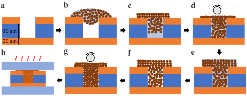
The microvia filling process employs distinct methods tailored to material type and production scale. Copper filled microvias rely on electrolytic plating, starting with electroless copper seed layer deposition after laser drilling and desmear. Pulse reverse electroplating then fills the via from bottom to top, minimizing voids through controlled current density and reversal. This super-filling technique creates a slight dome or flat top, which lamination flattens. Epoxy filled microvias use screen printing or vacuum-assisted dispensing to inject paste into vias, followed by thermal curing.
For copper filling, the process sequence includes panel electroplating for initial barrel plating before targeted via filling. Reverse pulse plating parameters adjust additive concentrations to promote uniform growth. Epoxy methods accommodate higher aspect ratios since paste flows under pressure, but require stencil design for precision. Hybrid approaches combine conductive paste with plating for through-hole filling in complex boards. Factories optimize these methods per IPC guidelines to achieve consistent results across panels.
Conductive pastes for epoxy filled microvias incorporate metal flakes suspended in resin, screened through fine meshes matching via pitch. Curing schedules align with board bake-out to prevent outgassing. Copper methods demand cleanroom controls to avoid contamination during plating baths. Both approaches cap filled vias with photoresist or dielectric for protection.
Detailed Microvia Filling Process
The microvia filling process begins with precise laser ablation using UV or CO2 lasers to form vias in dielectric layers. Desmear removes resin smear via plasma or permanganate etching, ensuring a clean barrel for metallization. For copper filled microvias, electroless plating deposits a thin conductive layer, followed by graphic electroplating to thicken walls. The filling phase employs periodic pulse reverse (PPR) plating, where anode dissolution during reverse current enhances ion replenishment and suppresses dendrite formation. Post-filling, planarization via chemical mechanical polishing (CMP) achieves surface flatness.
Epoxy filling follows a simpler workflow: paste screening through stencils aligned to fiducials, vacuum assistance for deep fills, and oven curing at controlled ramps. Inspection via automated optical or x-ray verifies fill completeness, detecting voids larger than 10% of via area. Sequential lamination builds additional layers over filled vias, with via capture pad overlap per design rules. Process controls monitor bath chemistry, temperature, and agitation for reproducibility. As per IPC-2226, aspect ratios influence fill success, guiding method selection.
Reliability Considerations in Microvia Filling
Microvia filling reliability hinges on void-free fills, plating uniformity, and material interactions under stress. Copper filled microvias excel in thermal cycling due to matched CTE with copper traces, reducing crack propagation risks. Epoxy fills risk delamination from CTE mismatch with dielectrics, especially in stacked vias exposed to reflow peaks. Voids act as stress concentrators, accelerating fatigue during interconnect stress testing (IST). Plating defects like overplating or underfill compromise current carrying capacity and heat transfer.
Reliability testing per IPC-TM-650 methods evaluates filled microvias under thermal shock, vibration, and humidity. Copper fills demonstrate higher cycle life in high-power applications owing to better conductivity. Epoxy variants suit signal layers where insulation suffices, but require low-modulus resins for flexibility. Stacking multiple filled microvias amplifies risks, demanding robust fill quality. Factory data correlates fill density over 95% with passing HAST and thermal cycle qualifications.
Warpage from uneven filling affects panel yield, mitigated by symmetric stacking. Reliability models predict lifetime based on via geometry and material properties. Engineers specify fill type per IPC-6012 performance classes to align with end-use environments.
Best Practices for PCB Microvia Filling
Implement design rules limiting microvia aspect ratios to ensure reliable filling, favoring shallower depths for epoxy methods. Specify copper filled microvias for stacked or power vias, reserving epoxy for non-critical signals. Collaborate with fabricators early to validate process capabilities via test coupons. Monitor plating bath parameters to maintain additive balance, preventing fill inconsistencies. Post-fill x-ray and cross-section analysis confirm quality before lamination.
Optimize stencil thickness and aperture design for epoxy screening, achieving squeegee pressure uniformity. Bake boards pre-filling to remove moisture, averting voids during cure. For copper processes, sequence panel and pattern plating to control thickness. Adhere to IPC standards for acceptance criteria, classifying fills per performance levels. These practices reduce defects, enhancing microvia filling reliability in production.
Conclusion
PCB microvia filling remains essential for advancing HDI PCB capabilities, with copper and epoxy methods offering tailored solutions for diverse needs. Copper filled microvias provide unmatched conductivity for demanding applications, while epoxy filled microvias enable cost-effective planarization. The microvia filling process demands precision in drilling, plating, and inspection to achieve void-free results. Reliability considerations guide material selection, ensuring endurance under thermal and mechanical stresses. By following best practices aligned with industry standards, engineers secure robust interconnects for next-generation electronics.
FAQs
Q1: What are the main differences between copper filled microvias and epoxy filled microvias?
A1: Copper filled microvias use electroplating for full metallic conductivity and superior heat transfer, ideal for stacked vias and high-current paths. Epoxy filled microvias employ paste screening for faster, lower-cost processing, suitable for signal layers with insulation needs. Copper offers better reliability in thermal cycling due to CTE matching, while epoxy risks mismatch issues if not formulated properly. Factories select based on design density and performance class per IPC guidelines. Overall, copper suits premium HDI boards.
Q2: How does the microvia filling process impact PCB reliability?
A2: The microvia filling process directly affects void formation, plating uniformity, and stress distribution, key to microvia filling reliability. Incomplete fills create crack initiation sites during reflow or operation. Copper processes ensure planar surfaces for fine-line imaging, epoxy provides mechanical plug strength. Testing via IPC-TM-650 verifies endurance. Proper execution minimizes failures in stacked configurations.
Q3: When should engineers specify PCB microvia filling in designs?
A3: Specify PCB microvia filling for via-in-pad BGAs, stacked microvias, or applications needing planarity for 2-mil lines. It prevents solder entrapment and enhances thermal management. Use copper for power integrity, epoxy for cost-sensitive signals. Align with IPC-2226 rules for aspect ratios. Essential in HDI classes 3 and above.
Q4: What factors influence microvia filling reliability in manufacturing?
A4: Key factors include via geometry, material CTE compatibility, and process controls like pulse plating parameters. Voids from poor desmear or bath imbalance degrade performance. Stacking amplifies risks, requiring 100% fill verification. Standards like IPC-6012 define acceptance. Factories prioritize these for high-yield production.
References
IPC-2226 — Design Standard for High Density Interconnects. IPC.
IPC-6012E — Qualification and Performance Specification for Rigid Printed Boards. IPC, 2015.
IPC-TM-650 2.6.26 — Interconnect Stress Test. IPC.