Introduction
PTFE PCBs represent a cornerstone in high-frequency applications where signal integrity demands the utmost precision. Polytetrafluoroethylene, known for its exceptional electrical properties, enables designs that operate effectively in RF and microwave environments. Designing the stackup for these boards requires careful consideration of material characteristics and layer arrangements to achieve reliable performance. This guide explores the intricacies of PTFE PCB stackup impedance, PTFE PCB layer thickness, and PTFE PCB controlled impedance, providing engineers with structured insights for optimal results. By understanding these elements, designers can mitigate common pitfalls and enhance overall circuit functionality.
Engineers often face challenges in balancing cost, manufacturability, and performance when specifying PTFE materials. The stackup defines not just the physical build but also the electrical behavior of traces and vias. Proper design ensures minimal signal loss and distortion, critical for applications like radar systems and telecommunications. This article draws on established engineering principles to deliver actionable strategies.
What Is PTFE PCB Stackup and Why It Matters
A PTFE PCB stackup refers to the sequential arrangement of conductive layers, dielectrics, and cores that form the multilayer structure of the board. In PTFE-based designs, this stackup must account for the material's unique properties, such as low dielectric constant and minimal loss tangent, which are essential for high-frequency signal propagation. Unlike standard FR4 stackups, PTFE configurations prioritize symmetry to prevent warpage and maintain dimensional stability during fabrication and assembly.
The relevance of PTFE PCB stackup design stems from its direct impact on electrical performance. Impedance mismatches can lead to reflections and attenuation, degrading signal quality in sensitive circuits. Engineers must optimize the stackup to support controlled impedance traces, ensuring predictable transmission line behavior. Furthermore, precise layer arrangements influence thermal management and mechanical integrity, making stackup a foundational aspect of reliable PCB design.
In high-speed applications, neglecting stackup details results in costly redesigns and performance failures. Industry standards like IPC-2221 provide guidelines for generic printed board design, emphasizing the need for balanced layer configurations. This structured approach allows electrical engineers to predict and verify performance early in the design cycle.
Technical Principles of PTFE PCB Stackup Design
Fundamentals of Impedance in PTFE Stackups
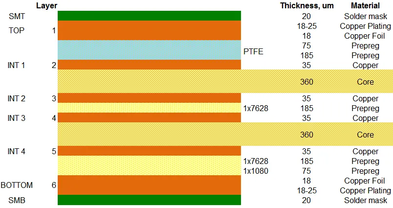
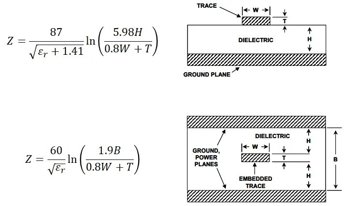
PTFE PCB stackup impedance arises from the interaction between trace geometry, dielectric properties, and layer spacing. The characteristic impedance of a transmission line depends primarily on the dielectric constant and the effective distance between signal and reference planes. In PTFE materials, the consistently low dielectric constant facilitates higher impedance values or narrower traces compared to higher-Dk substrates, aiding compact designs.
Controlled impedance requires modeling the stackup accurately, considering both microstrip and stripline configurations. Microstrips, positioned on outer layers, expose signals to air, altering effective dielectric constants, while striplines embed traces between ground planes for better shielding. Engineers calculate impedance using field solvers that incorporate stackup parameters, ensuring tolerances align with application requirements.
Symmetry in the stackup prevents uneven expansion due to PTFE's high coefficient of thermal expansion. Balanced cores and prepregs around the neutral axis minimize bow and twist. This principle extends to via transitions, where stub lengths must be controlled to avoid resonance at operating frequencies.
Role of Layer Thickness in PTFE PCBs
PTFE PCB layer thickness directly influences impedance control and signal integrity. Dielectric thickness between signal and ground planes determines the electric field distribution, with thinner layers enabling tighter impedance control but increasing capacitive coupling risks. Thicker layers reduce coupling but demand wider traces to maintain impedance, impacting routing density.
Fabrication tolerances for PTFE layers demand precision because small variations amplify impedance deviations. Engineers specify thicknesses based on frequency needs, balancing manufacturing capabilities with performance goals. Hybrid stackups, combining PTFE with compatible resins, allow finer control over core and prepreg thicknesses.
Adherence to standards like IPC-6012 for qualification and performance of rigid printed boards ensures layer thicknesses meet reliability criteria. Variations in thickness can shift resonance frequencies, underscoring the need for consistent material selection and process controls.
Material Interactions and Dielectric Properties
PTFE's low loss tangent minimizes energy dissipation, making it ideal for broadband applications. However, pure PTFE poses processing challenges, often requiring filled composites to improve mechanical properties without compromising electrical performance. Stackup design must integrate these hybrids thoughtfully, placing high-frequency signals on pure PTFE layers.
Dielectric constant stability across frequencies and temperatures is crucial for PTFE PCB controlled impedance. Environmental factors like humidity affect absorption, so stackups incorporate barriers or sealed enclosures. Vias and planes interact with dielectrics, necessitating back-drilling or blind vias to preserve impedance continuity.
Best Practices for PTFE PCB Stackup Design
Start with a symmetrical stackup to counteract PTFE's anisotropic expansion. Position signal layers adjacent to ground planes for return path proximity, reducing inductance and radiation. Dedicate inner layers to power distribution with wide planes, segmented to manage currents and minimize noise.
For PTFE PCB stackup impedance, employ consistent trace widths and spaces across nets requiring matching. Use 50-ohm single-ended or 100-ohm differential pairs as baselines, adjusting geometries iteratively via simulation. Validate with time-domain reflectometry post-fabrication.
Optimize PTFE PCB layer thickness by minimizing the number of dielectric types while achieving target impedances. Thin cores for high-density interconnects pair with thicker prepregs for rigidity. Collaborate with fabricators early to confirm achievable tolerances.
Incorporate thermal vias and embedded heat spreaders in stackups handling high power. Plane splits should avoid signal crossings to prevent impedance discontinuities. Finalize designs with stackup drawings specifying foil weights, core types, and press cycles.
Common Challenges and Troubleshooting in PTFE Stackups
Warpage remains a primary challenge due to CTE mismatches in PTFE stackups. Mitigation involves symmetric builds and controlled lamination cycles. Measure warpage per IPC-TM-650 methods to verify compliance.
Impedance variations from plating or etching tolerances require over-specification margins. Troubleshoot with coupon tests on production panels. Hybrid materials introduce Dk gradients; model accordingly.
Via resonance plagues high-frequency PTFE designs. Shorten stubs or use depth-controlled drilling. Signal skew in asymmetric stacks demands length matching and serpentine routing.
Conclusion
Mastering PTFE PCB stackup design hinges on integrating impedance control, layer thickness optimization, and material symmetry. These elements ensure low-loss propagation and mechanical reliability in demanding applications. Engineers benefit from iterative simulation and standards adherence, like IPC-4103 for high-frequency materials, to achieve first-pass success. Prioritize collaboration with manufacturing partners to translate designs into high-performance boards. This approach not only meets specifications but elevates overall system efficiency.
FAQs
Q1: What factors most influence PTFE PCB stackup impedance?
A1: PTFE PCB stackup impedance depends on dielectric thickness, trace width, and reference plane proximity. Low dielectric constant in PTFE allows precise control, but tolerances in layer thickness can cause variations. Simulations incorporating full stackup details ensure targets like 50 ohms are met reliably. Adhering to design guidelines prevents reflections in high-speed signals.
Q2: How do you select optimal PTFE PCB layer thickness?
A2: Choose PTFE PCB layer thickness based on impedance requirements and routing density. Thinner dielectrics support tighter control but risk crosstalk; thicker ones enhance isolation. Balance with fabrication tolerances and thermal needs. Verify through stackup calculators for consistent performance across frequencies.
Q3: Why is controlled impedance critical in PTFE PCB designs?
A3: PTFE PCB controlled impedance minimizes signal reflections and losses in RF applications. It maintains waveform integrity by matching transmission line characteristics to driver and receiver impedances. Stackup symmetry and precise geometries achieve this. Neglect leads to attenuation and crosstalk issues.
Q4: What are common pitfalls in PTFE PCB stackup design?
A4: Asymmetric stackups cause warpage, while mismatched dielectrics disrupt impedance. Overlooking via effects introduces resonances. Start with symmetric builds and hybrid materials for stability. Test coupons confirm PTFE PCB controlled impedance before full production.
References
IPC-2221B — Generic Standard on Printed Board Design. IPC, 2012
IPC-6012E — Qualification and Performance Specification for Rigid Printed Boards. IPC, 2015
IPC-4103D — Specification for Base Materials for High Speed/High Frequency Applications. IPC, 2015