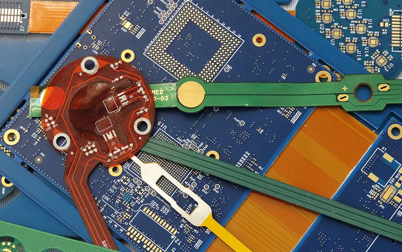
In the current era of advanced electronic hardware, Rigid-Flex PCB Manufacturing represents the pinnacle of interconnect technology. As devices shrink in size while growing in computational power, traditional cabling and rigid boards are no longer sufficient. Rigid-flex technology offers a seamless, three-dimensional hybrid solution that integrates the structural stability of rigid circuits with the versatility of flexible polyimide sections.
However, the path from a digital design to a high-yield physical product is fraught with technical hurdles. Rigid-flex manufacturing is a multidisciplinary challenge requiring mastery of material science, mechanical stress analysis, and high-precision chemical processes. This guide serves as a comprehensive technical blueprint, exploring the full lifecycle of rigid-flex production—from engineering precision to global volume scaling.
1. The Strategic Foundation: Why Rigid-Flex?
Rigid-flex boards are more than just a combination of two materials; they are integrated systems that solve mechanical and electrical problems simultaneously. By eliminating connectors and wire harnesses, rigid-flex manufacturing:
-
Reduces Total System Weight: Vital for aerospace and portable medical devices.
-
Enhances Signal Integrity: Continuous copper paths across rigid and flex zones minimize impedance mismatches.
-
Increases Reliability: Eliminating solder joints at connectors removes the primary point of failure in electronic systems.
-
Enables 3D Packaging: Allows "origami-style" folding to fit into non-rectangular or ultra-slim enclosures.
2. Advanced Material Science in Rigid-Flex Production
The reliability of a rigid-flex board depends entirely on its base materials. Manufacturers must balance the rigid FR4 sections with flexible Polyimide (PI) cores.
Adhesiveless Laminates
Modern high-end manufacturing has shifted away from adhesive-based systems. Adhesiveless polyimide is now the gold standard. By removing the acrylic or epoxy adhesive layer, manufacturers can produce thinner, more flexible boards with superior thermal stability. Adhesives often have high moisture absorption and high Coefficients of Thermal Expansion (CTE), which can lead to via cracking during lead-free soldering. Adhesiveless materials mitigate these risks.
Copper Selection: RA vs. ED
The choice of copper foil is determined by the application’s mechanical requirements. While Electro-Deposited (ED) copper is standard for rigid sections, Rolled Annealed (RA) copper is mandatory for flexible zones intended for dynamic movement. RA copper’s grain structure is aligned horizontally, allowing it to withstand millions of flex cycles without work-hardening or fracturing.
3. Engineering Challenges: Managing High-Density Layouts
As component density increases, the manufacturing process must adapt to handle tighter tolerances and sophisticated electrical requirements.
Thermal Dynamics and Heat Dissipation
One of the most significant hurdles in high-density manufacturing is managing the heat generated by high-power components. Because polyimide and FR4 have different thermal conductivity levels, localized "hotspots" can lead to material delamination or signal degradation. High-reliability manufacturing requires solving thermal management challenges in high-density rigid-flex PCB manufacturing. This involves implementing innovative heat dissipation techniques such as thermal vias, heavy copper layers, and specialized dielectrics to ensure long-term system stability under high-power loads.
Signal Integrity and Impedance
In a hybrid environment, maintaining a consistent 50-ohm or 100-ohm environment is a precision task. The transition zone—where the board changes from FR4 to Polyimide—requires manual adjustments to trace widths to account for the different Dielectric Constants (Dk) of the materials.
4. The Manufacturing Lifecycle: From Concept to Volume
The journey of a rigid-flex product is a multi-stage evolution. A design that works for a single prototype may not be viable for a production run of 100,000 units.
The Prototype Phase
Prototyping is essential for verifying 3D mechanical fit and signal performance. During this phase, manufacturers focus on rapid turnaround and testing the "bendability" of the circuit.
Scaling for Commercial Success
Transitioning to volume requires a shift in focus toward "Yield Optimization" and "Cost-Effective Panelization." This stage involves a rigorous Design for Manufacturability (DFM) review to ensure the board can be built reliably using high-speed automated equipment. Successfully bringing a product to market depends on scaling up your rigid-flex PCB manufacturing from prototype to production, a process centered on yield optimization and cost-effective volume manufacturing to bridge the gap between innovation and commercial reality.
5. The Manufacturing Process Deep-Dive
The production of a rigid-flex board is a sequential and highly controlled process.
Step 1: Flex Layer Etching and LDI
Flexible layers are processed first. Due to the dimensional instability of polyimide, Laser Direct Imaging (LDI) is used to ensure that traces are registered with micron-level accuracy.
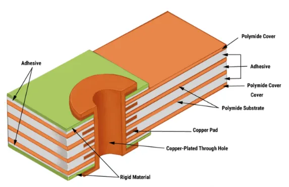
Step 2: Coverlay Lamination
Instead of liquid solder mask, flexible sections are protected by a Coverlay. This polyimide sheet is laminated under heat and pressure, providing a durable, flexible barrier against oxidation and moisture.
Step 3: Sequential Lamination and No-Flow Prepreg
The rigid and flex layers are "sandwiched" together. Manufacturers must use no-flow prepreg to prevent resin from leaking onto the flexible "wings" of the board, which would render the circuit brittle and prone to failure during the first bend.
Step 4: Drilling and Plasma Desmear
Mechanical or laser drilling creates vias. However, the heat of the drill often causes "resin smear." Because chemical desmearing can be too aggressive for polyimide, high-end facilities utilize Plasma Etching. Plasma gas cleans the via holes at a molecular level, ensuring a perfect copper-to-copper bond.
6. Quality Assurance and Mission-Critical Testing
Because rigid-flex PCBs are often used in medical implants, aerospace avionics, and high-stakes industrial equipment, quality control is paramount.
-
AOI (Automated Optical Inspection): Scans the inner layers for defects before lamination.
-
Flying Probe Testing: Verifies electrical continuity in a 3D environment.
-
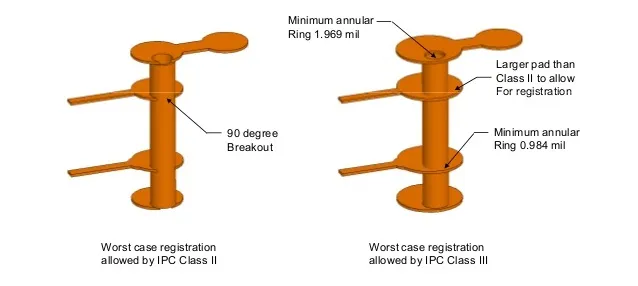
X-Ray Inspection: Checks the internal registration of the 10+ layers to ensure vias are aligned with their pads.
-
Micro-sectioning: Destructive testing on coupons to verify plating thickness and material bonding.
7. Future Trends: The Next Frontier of Rigid-Flex
As we look toward the next decade, Rigid-Flex PCB Manufacturing is evolving beyond traditional subtractive etching into the realm of semi-additive and biocompatible technologies. One of the most transformative shifts is the rise of Ultra-HDI (High-Density Interconnect) via mSAP (modified Semi-Additive Process). As 5G and AI hardware demand trace widths below 25 microns, mSAP allows manufacturers to "grow" copper traces with vertical sidewalls, offering far superior signal integrity and density than chemical etching could ever achieve.
Furthermore, the industry is seeing a transition in materials. While Polyimide remains the standard, Liquid Crystal Polymer (LCP) is emerging as a high-frequency alternative for 6G and millimeter-wave applications due to its near-zero moisture absorption and lower dielectric loss. We are also entering an era of "Functional Substrates," where embedded active components—such as resistors and silicon dies—are placed inside the inner layers during the lamination process. This turns the PCB from a mere mounting board into a fully integrated electronic component. Additionally, as wearable technology moves into "smart fabrics" and medical biosensors, the manufacturing of biocompatible, ultra-thin rigid-flex boards is becoming a standalone discipline, requiring cleanroom environments and specialized gold-based finishing processes to ensure safety within the human body.
8. Conclusion
Rigid-Flex PCB Manufacturing is the cornerstone of modern electronic innovation. By mastering the complexities of thermal management and understanding the strategic requirements of scaling from prototype to production, manufacturers can deliver products that are not only smaller and lighter but significantly more reliable. As this technology matures, it will continue to unlock new possibilities in IoT, 5G, and beyond.
FAQs
Q1: What are the main cost drivers in Rigid-Flex Manufacturing?
A1: The primary drivers are material costs (Polyimide and RA copper are far more expensive than FR4), the labor-intensive sequential lamination process, and the lower yield rates compared to standard rigid PCBs. Strategic DFM can help mitigate these costs during the scaling phase.
Q2: How does Plasma Etching improve board reliability?
A2: Standard chemical desmearing can be too harsh for polyimide, leading to delamination. Plasma etching uses ionized gas to clean the via holes precisely, providing a superior surface for copper plating and ensuring the via-to-trace connection remains intact during thermal cycling.
Q3: Is Rigid-Flex manufacturing suitable for high-speed signals?
A3: Yes. Rigid-flex is ideal for high-speed signals because it eliminates connectors that cause signal reflection. However, it requires expert impedance control at the rigid-to-flex transition zones due to the varying dielectric constants of the materials.