Introduction
Thermal relief structures play a critical role in printed circuit board (PCB) design, particularly when connecting pads to large copper planes. These features address the challenges of heat transfer during soldering processes, ensuring reliable assembly outcomes. In high-density boards with power and ground planes, direct pad-to-plane connections can lead to excessive heat sinking, complicating reflow soldering. Engineers must balance electrical connectivity, thermal management during assembly, and long-term performance. This article explores thermal relief design rules, practical implementation for connecting pads to planes, and strategies for preventing tombstoning while improving solder joint reliability.
What Is Thermal Relief and Why It Matters
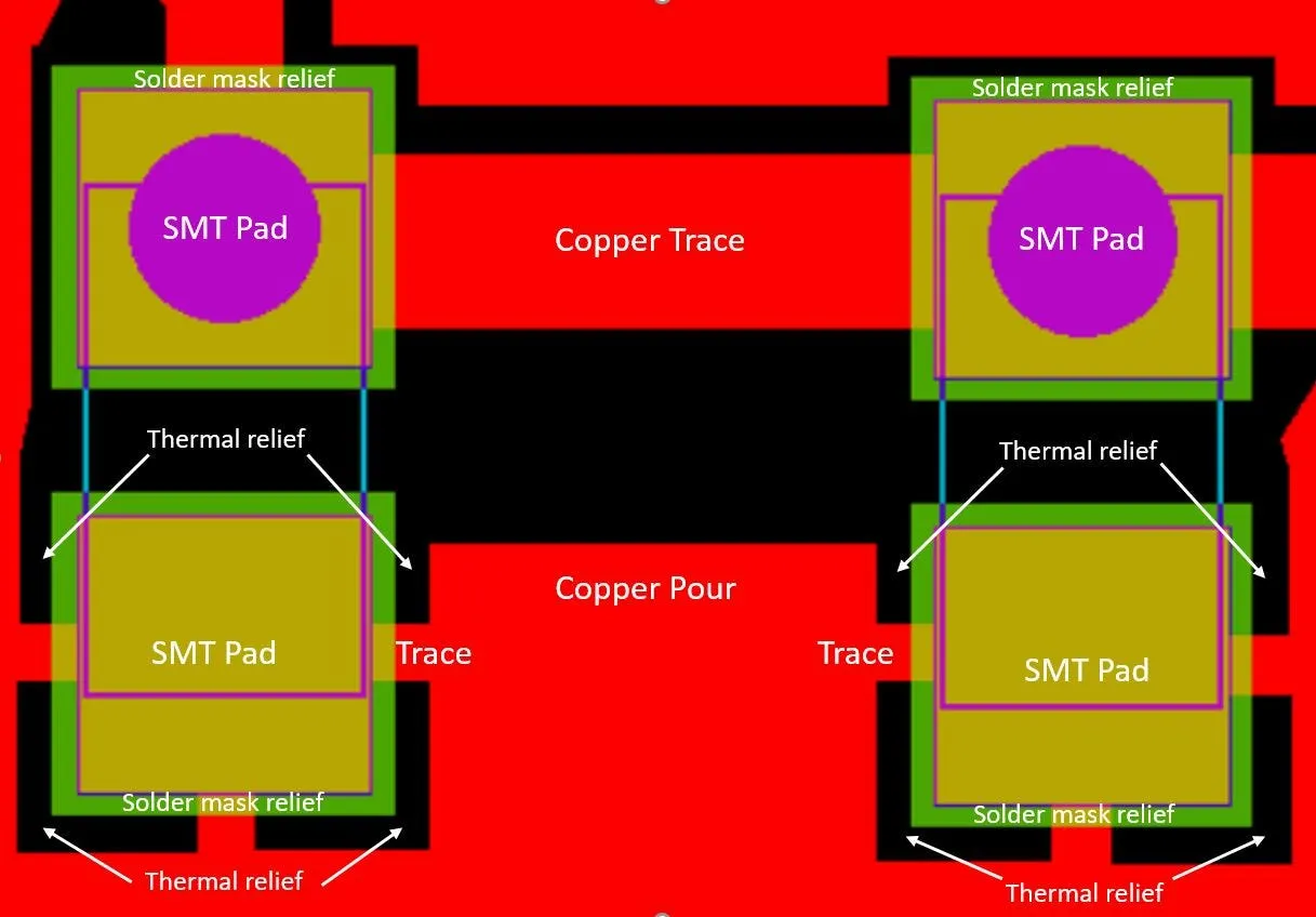
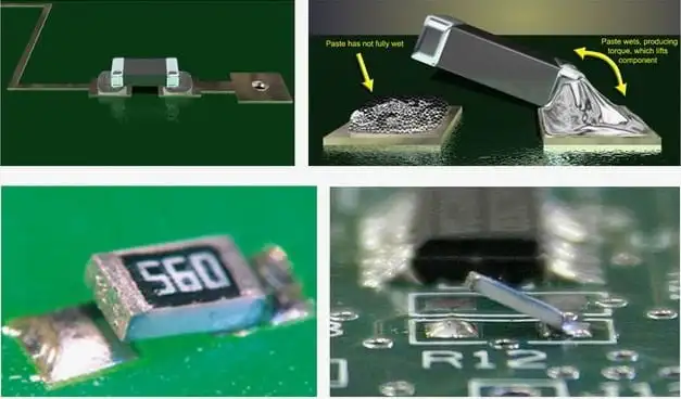
Thermal relief refers to a patterned connection between a component pad and a surrounding copper plane, typically consisting of narrow spokes separated by clearances. This design intentionally increases thermal resistance compared to a full solid connection, allowing localized heating of the pad during soldering. Without thermal relief, the plane acts as a massive heat sink, rapidly dissipating heat from the solder joint and prolonging reflow times. This can result in incomplete wetting, cold joints, or defects like tombstoning in surface-mount devices.
The relevance extends to modern electronics where multilayer boards feature extensive power planes for efficient current distribution. Proper thermal relief ensures consistent solder joint formation across varied component types and plane thicknesses. It directly impacts assembly yield, rework feasibility, and overall board reliability. For electric engineers, understanding these principles prevents field failures linked to marginal solder joints under thermal cycling.
Technical Principles of Thermal Relief
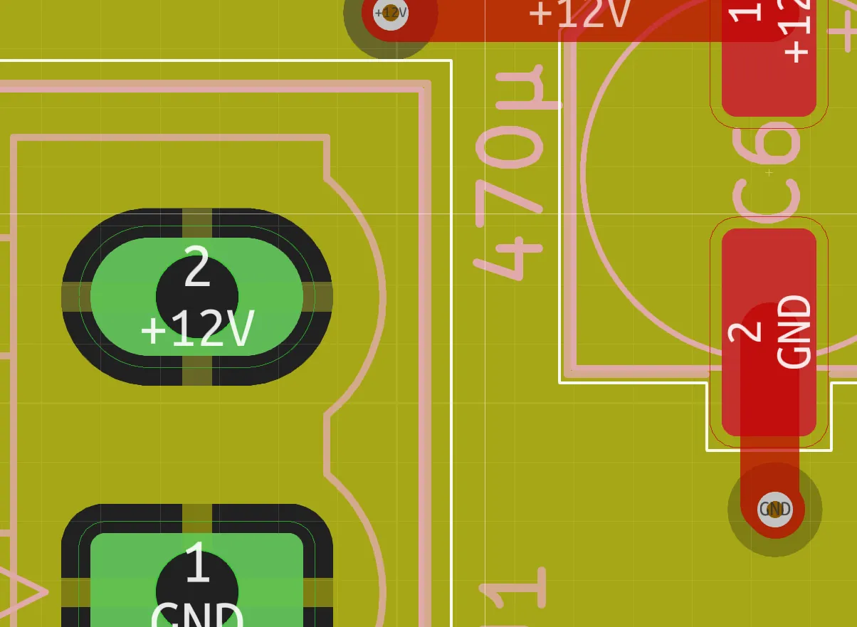
Heat transfer in PCB soldering follows conduction principles, where the rate depends on the contact area and material properties. A solid pad-to-plane connection maximizes thermal conductivity, drawing heat away faster than it can melt the solder alloy. Thermal relief introduces spokes that limit this path, creating a thermal bottleneck that confines heat to the pad. Typically, spokes are arranged radially, often four at 90-degree intervals, with widths and gaps tuned to the application's needs.
The thermal resistance of the relief structure scales inversely with spoke width and number. Narrower spokes increase resistance, aiding hand soldering, while wider ones support higher current post-assembly. Copper's high thermal conductivity, around 400 W/m·K, amplifies the effect of large planes, necessitating relief for pads larger than minimal sizes. Finite element simulations confirm that spoke geometry significantly influences peak pad temperatures during reflow profiles.
Preventing tombstoning hinges on symmetrical heating across component leads. Uneven heat dissipation, common with direct plane connections on one side, causes premature solder liquefaction on the plane side, lifting the free end. Thermal relief symmetrizes this by throttling plane heat sinking equally. Standards like IPC-2221 provide generic guidelines for such plane connection patterns to ensure manufacturability.
Key Factors in Thermal Relief Design Rules
Thermal relief design rules center on spoke dimensions, gap sizes, and pad geometry compatibility. Spoke width should align with the trace width required for the net's current-carrying capacity, ensuring post-soldering electrical performance matches design intent. Common practice sets spoke widths from 0.1 mm to 0.5 mm, depending on layer copper weight and power levels, though exact values derive from simulation or empirical testing. Gaps between spokes, often 0.2 to 0.4 mm, further tune thermal isolation without compromising etchability.
Connecting pads to planes demands consideration of board stackup and plane location. Inner layer planes require via-in-pad relief if through-hole components are used, but surface pads benefit from direct spoke patterns. For high-power applications, multiple spokes maintain low resistance while providing relief. Engineers evaluate these via thermal modeling tools, correlating spoke parameters to reflow oven profiles.
The interplay of spoke width and count affects both assembly and reliability. Fewer spokes enhance relief but risk higher resistance; more spokes improve conductivity at the cost of reduced isolation. Optimal configurations emerge from balancing these trade-offs.
Best Practices for Connecting Pads to Planes
Implement thermal relief selectively, applying it to pads interfacing with planes larger than 5 mm2 to avoid unnecessary complexity on signal nets. For surface-mount technology (SMT), use four-spoke patterns on power planes to standardize heating. When connecting pads to planes, verify solder mask openings align precisely with pad edges to prevent bridging across spokes. This practice supports consistent reflow and minimizes defects.
Thermal relief spoke width optimization starts with current calculations per IPC-2221 thermal management sections. Match spoke total cross-section to the incoming trace to preserve ampacity. For example, a 1 mm trace might use four 0.25 mm spokes. Test prototypes under actual reflow conditions to validate joint fillet formation and voiding levels.
Preventing tombstoning involves symmetrical relief on opposing pads of chip components. Apply identical spoke geometries to both ends, especially for 0402 or smaller parts on dense planes. Additional measures include stencil aperture reductions for paste volume control. These steps enhance assembly robustness across production runs.
Improving solder joint reliability extends beyond assembly to operational life. Thermal relief reduces intermetallic compound growth variations from uneven heating, promoting uniform microstructure. Under accelerated thermal cycling, joints with optimized relief exhibit lower crack propagation rates. Pair this with via thermal relief for multilayer heat paths.
J-STD-001 outlines acceptance criteria for soldered connections, emphasizing fillet coverage and wetting around relief spokes. Compliance ensures joints withstand vibration and temperature excursions.
Troubleshooting Common Thermal Relief Issues
Designers encounter challenges like insufficient relief causing prolonged reflow dwells or excessive relief leading to high resistance. Diagnose by monitoring peak pad temperatures with thermocouples during profiling. If tombstoning persists, widen gaps or reduce spoke count incrementally. Verify etch factor post-fabrication, as under-etching merges spokes unintentionally.
For high-current nets, post-assembly resistance checks reveal if spoke widths suffice. Rework direct connections to relief patterns using hot air if needed, but prioritize upfront design. Simulate airflow in reflow ovens to predict plane cooling effects on outer layers.
Conclusion
Thermal relief optimizes pad-to-plane connections by managing heat during soldering, directly addressing tombstoning and reliability concerns. Adhering to thermal relief design rules, including spoke width selection, yields robust assemblies. Engineers benefit from structured approaches balancing assembly ease with performance. Integrating these practices elevates PCB quality, reducing defects and enhancing longevity.
FAQs
Q1: What are the key thermal relief design rules for connecting pads to planes?
A1: Thermal relief design rules emphasize spoke widths matching trace ampacity and gaps of 0.2-0.4 mm for thermal isolation. Use 2-4 spokes radially to throttle heat sinking during reflow. Align patterns symmetrically for chip components to prevent uneven heating. These rules, informed by IPC-2221, ensure manufacturable connections without compromising conductivity.
Q2: How does thermal relief help in preventing tombstoning?
A2: Thermal relief symmetrizes heat dissipation across component pads connected to planes, avoiding rapid cooling on one side. Narrow spokes limit plane heat sinking, allowing uniform solder melting. This reduces lift-off risks in small SMDs like 0402 parts. Consistent application improves assembly yields significantly.
Q3: What is the optimal thermal relief spoke width for improving solder joint reliability?
A3: Thermal relief spoke width should equal the trace width for the net's current needs, typically 0.15-0.3 mm for standard applications. Wider spokes support power delivery while providing relief. This maintains low resistance post-reflow and uniform joint formation. Validation through profiling confirms reliability gains.
Q4: When should thermal relief be avoided in PCB design?
A4: Avoid thermal relief on signal traces or small planes under 5 mm2, where full connections suffice without heat issues. Direct connects suit low-power nets for maximal conductivity. Reserve relief for large power/ground planes interfacing component pads. Assess via thermal simulation for borderline cases.
References
IPC-2221C — Generic Standard on Printed Board Design. IPC, 2022
IPC-7352 — Generic Guideline for Land Pattern Design. IPC, 2023
J-STD-001H — Requirements for Soldered Electrical and Electronic Assemblies. IPC, 2020