Introduction
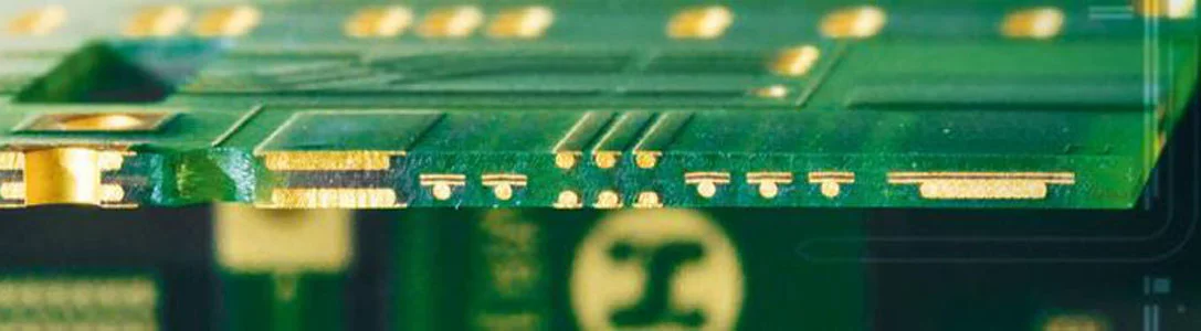
Electric vehicles demand robust electronics to manage high power levels and ensure safety under demanding conditions. Thick copper PCBs play a critical role in handling the substantial currents and voltages found in EV systems. These boards feature copper layers significantly thicker than standard designs, enabling better thermal dissipation and current-carrying capacity. In applications like battery management systems and charging infrastructure, thick copper PCB manufacturing becomes essential for reliability. Automotive PCB manufacturing processes must align with stringent quality controls to meet the rigors of EV deployment. This article explores the principles, processes, and best practices for producing these specialized boards.
What Are Thick Copper PCBs and Why Do They Matter in EVs?
Thick copper PCBs incorporate copper weights that exceed conventional levels, typically used where high current density is required. Factory processes start with selecting appropriate copper foils and substrates capable of withstanding the mechanical stresses of lamination. In EVs, these boards support power distribution in inverters, converters, and control units, where standard thin copper would overheat or fail prematurely. The enhanced cross-sectional area of thick copper traces reduces resistance and voltage drop, crucial for efficient energy transfer. Manufacturers prioritize these designs to address the growing power demands of modern EV architectures. Compliance with IPC-6012 qualification specifications ensures the boards meet performance benchmarks for rigid printed boards.
Thick copper PCB reliability in EVs hinges on their ability to manage heat generated by high currents without compromising structural integrity. During operation, EV components experience thermal cycling, vibration, and humidity, all of which test the board's endurance. Factory-driven insights reveal that thicker copper improves mechanical strength, reducing the risk of trace fractures over time. Engineers specify these boards for critical paths where current loads exceed what lighter copper can handle safely. The shift toward higher voltage systems in EVs further underscores the need for such robust constructions. Proper selection prevents hotspots that could lead to system failures.
Key Design Principles for High Voltage PCB Design
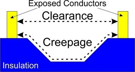
High voltage PCB design requires careful attention to isolation distances and material choices to prevent arcing or breakdown. Thick copper layers demand wider traces and adjusted spacing to accommodate differential etching during fabrication. Designers must calculate creepage and clearance based on voltage ratings, incorporating slots or barriers where necessary. Substrate materials with high glass transition temperatures support the thermal expansion mismatch between thick copper and dielectrics. In automotive PCB manufacturing, simulations verify that designs maintain integrity under peak loads. Adhering to IPC-2221 guidelines for printed circuit board design aids in determining appropriate trace geometries for current handling.
Multilayer configurations amplify challenges, as sequential lamination bonds heavy copper cores with prepregs under high pressure. Vias plated to match copper thickness ensure reliable interconnections without bottlenecks. High voltage sections benefit from embedded resistors or capacitors for filtering, integrated directly into the thick copper structure. Factory processes emphasize uniform plating to avoid voids that could propagate under electrical stress. Testing protocols simulate EV conditions, confirming dielectric withstand voltage exceeds operational margins. These principles ensure the board supports the EV's power electronics ecosystem effectively.
Manufacturing Processes in Automotive PCB Manufacturing
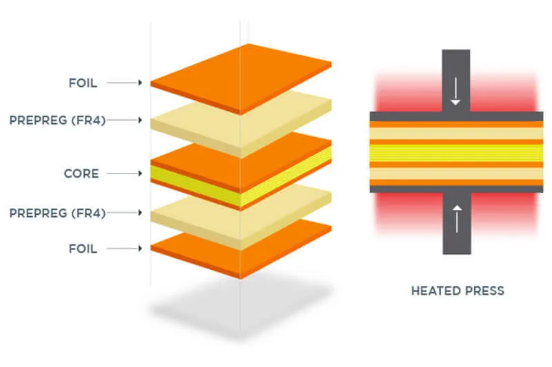
Automotive PCB manufacturing for thick copper begins with panel preparation, where heavy copper foils are laminated onto cores using controlled heat and pressure cycles. Differential etching techniques remove excess copper selectively, preserving trace integrity despite varying thicknesses. Plated through-hole processes deposit additional copper to fill vias, matching the outer layer weights for balanced thermal performance. Successive lamination builds multilayers, with alignment critical to prevent misalignment in high-density areas. Factories employ X-ray inspection to verify via fill and barrel quality post-plating. These steps align with IPC-A-610 acceptability criteria for high-reliability assemblies.
Post-etching, surface finishes like ENIG or hard gold protect against oxidation while supporting soldering in power modules. Routing and scoring account for the board's increased rigidity from thick copper, minimizing warpage during depanelization. Bake-out processes remove moisture before final assembly, preventing delamination in humid EV environments. Quality control includes electrical testing for shorts and opens, plus thermal shock simulations. Manufacturers calibrate equipment for repeatability, ensuring each batch meets automotive demands. This factory-centric approach guarantees thick copper PCBs withstand real-world stresses.
Warpage control poses a significant challenge due to asymmetric copper distribution. Factories use constrained lamination fixtures and symmetric stackups to balance stresses. Post-lamination flattening via presses restores planarity before drilling. Measurements against IPC-A-600 acceptability standards verify bow and twist limits suitable for automated assembly. In EV production, flat boards prevent connector misalignment in battery packs. Ongoing process tweaks based on statistical process control enhance yield.
Thick Copper PCB for BMS and EV Charging Station PCB Applications
In battery management systems, thick copper PCB for BMS handles sensing currents from multiple cells while distributing balancing power. These boards integrate shunts and FETs directly on heavy traces, minimizing inductance for precise monitoring. High current paths connect to external busbars, requiring robust terminations resistant to vibration. Factory builds emphasize low-impedance layouts to support fast discharge rates in traction batteries. Reliability testing cycles boards through charge-discharge profiles, validating longevity.
EV charging station PCB designs face similar high-power needs, routing AC-DC conversion currents through thick copper planes. Onboard power supplies and relays demand boards that dissipate kilowatts without failure. Multiphase topologies benefit from interleaved thick copper layers for current sharing. Manufacturing includes impedance-controlled etching to maintain phase balance. Deployment in outdoor stations requires conformal coatings over thick copper for corrosion resistance. These applications highlight the synergy between design and production expertise.
Enhancing Thick Copper PCB Reliability in EVs
Thick copper PCB reliability in EVs depends on mitigating thermal-mechanical stresses throughout the lifecycle. Factories conduct accelerated life testing, exposing boards to temperature swings and humidity to predict field performance. Solder joint integrity under vibration is assessed via shake table simulations. Material selection favors low CTE dielectrics to match copper expansion. Vias reinforced with filled plating resist cracking from cycling. Comprehensive data logging refines processes for consistent outcomes.
Common failure modes include copper cracking from over-etching or delamination from poor adhesion. Preventive measures involve optimized developer chemistries and adhesion promoters. Reliability improves with blind and buried vias, reducing surface clutter on thick copper surfaces. Post-assembly bake stabilizes the stackup before potting in EV housings. Factory insights stress traceability from raw materials to shipment, enabling root-cause analysis. These practices extend service life in demanding EV environments.
Best Practices for Thick Copper PCB Production
Start with design reviews incorporating DFM checks for thick copper feasibility, focusing on etch factors and panel utilization. Sequential builds for extreme thicknesses allow intermediate inspections. Use high-Tg FR-4 or polyimide for cores to handle lamination temperatures. Employ step plating for vias to build thickness gradually, avoiding stress cracks. Final inspections include cross-section analysis for copper ductility.
Procurement teams should specify stackup drawings with copper weights per layer. Factories recommend prototypes to validate warpage before full runs. Implement flying probe testing for high-voltage isolation verification. Storage in dry nitrogen cabinets prevents oxidation pre-assembly. Collaboration between design and manufacturing teams accelerates iterations. These practices optimize automotive PCB manufacturing outcomes.
Conclusion
Thick copper PCBs enable EV systems to operate at peak efficiency and safety. From high voltage PCB design to rigorous factory processes, every step contributes to superior performance. Applications in BMS and charging stations demonstrate their versatility. Adhering to standards like IPC specifications ensures quality. Engineers benefit from understanding these manufacturing nuances for better specifications. Future EV advancements will rely even more on such reliable boards.
FAQs
Q1: What makes thick copper PCB for BMS suitable for high-current sensing in EVs?
A1: Thick copper PCB for BMS uses heavier traces to carry balancing currents without significant voltage drop or heating. Factory processes ensure uniform plating for low resistance paths. This supports accurate cell monitoring across large packs. Reliability stems from robust mechanical properties under thermal cycling. Designs follow standard guidelines for trace sizing.
Q2: How does high voltage PCB design impact EV charging station PCB manufacturing?
A2: High voltage PCB design dictates wider clearances and reinforced isolation in EV charging station PCB layouts. Manufacturing adjusts etching and lamination for thick copper compatibility. This prevents arcing during high-power conversion. Factories verify via high-pot testing. Overall, it enhances safety in stationary infrastructure.
Q3: Why is thick copper PCB reliability in EVs critical for automotive PCB manufacturing?
A3: Thick copper PCB reliability in EVs counters vibration, heat, and humidity stresses common in vehicles. Automotive PCB manufacturing incorporates warpage controls and thermal simulations. Standards guide qualification for long-term endurance. Factories focus on via fill and adhesion for failure prevention. This ensures uninterrupted power delivery.
Q4: What role do standards play in thick copper PCB manufacturing processes?
A4: Standards like IPC-6012 define performance specs for rigid boards in thick copper applications. They outline qualification tests for EV suitability. Manufacturing aligns with acceptability criteria from IPC-A-610. This standardizes quality across factories. Engineers rely on them for consistent results.
References
IPC-6012E — Qualification and Performance Specification for Rigid Printed Boards. IPC, 2017
IPC-2221B — Generic Standard on Printed Board Design. IPC, 2012
IPC-A-610H — Acceptability of Electronic Assemblies. IPC, 2019


