Introduction
High-power LED lighting systems demand robust thermal management to sustain efficiency and extend operational life. LEDs convert a significant portion of electrical energy into light, but the remaining energy manifests as heat at the junction, which must be dissipated effectively. Standard PCBs with thin copper layers often fall short in handling this thermal load, leading to elevated temperatures that reduce luminous efficacy and accelerate degradation. Thick copper PCBs address this challenge by leveraging copper's high thermal conductivity to spread and conduct heat away from critical components. These boards feature copper weights exceeding 2 ounces per square foot, providing a larger cross-sectional area for heat flow. Engineers designing LED drivers, streetlights, and industrial luminaires increasingly turn to thick copper PCB for LED applications to achieve reliable performance under demanding conditions.
The integration of thick copper enhances not only heat dissipation but also current-carrying capacity, making it ideal for power-intensive LED circuits. As LED power densities rise, conventional thermal solutions like heatsinks alone prove insufficient without optimized PCB substrates. This article delves into the principles, design strategies, and manufacturing considerations for thick copper PCBs in LED lighting, offering practical insights for electric engineers.
What Are Thick Copper PCBs and Why They Matter for LED Lighting
Thick copper PCBs are rigid boards where the finished copper thickness on outer or inner layers exceeds 2 ounces per square foot, typically ranging from 2 to 20 ounces. This contrasts with standard 1-ounce copper boards used in low-power applications. The increased copper volume lowers electrical resistance and improves thermal spreading, crucial for components generating substantial heat. In LED lighting, where high-power LEDs operate at currents exceeding several amperes, thick copper prevents localized hotspots that could compromise solder joints and component reliability.
The relevance stems from the thermal requirements of modern LEDs. High-power LEDs, such as those in COB or high-lumen modules, produce junction temperatures that must remain below specified thresholds to avoid color shift and lumen depreciation. Thick copper PCBs act as an extension of the heat sink, conducting heat laterally across the board and vertically through layers. Factory processes align with standards like IPC-6012 to ensure these boards meet performance specifications for rigid printed boards. Without adequate thermal pathways, LED systems suffer reduced mean time between failures, impacting overall system cost.
Engineers benefit from thick copper's ability to integrate seamlessly with existing FR4 laminates, avoiding the need for exotic substrates in many cases. This approach balances cost and performance, particularly in applications like automotive headlights or architectural lighting where space constraints limit external cooling. By prioritizing thick copper PCB for LED designs, teams achieve compliance with thermal budgets while simplifying assembly.
Technical Principles of Heat Dissipation in Thick Copper PCBs
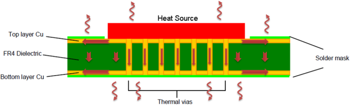
Copper's thermal conductivity, far superior to FR4 substrate materials, forms the foundation of effective heat dissipation in these PCBs. Heat from the LED junction flows through the thermal pad into the copper plane, where the thickness determines the conduction path's efficiency. Thicker copper increases the cross-sectional area, reducing thermal resistance according to Fourier's law of conduction. This mechanism allows heat to spread uniformly, minimizing temperature gradients across the board.
In multilayer configurations, heat transfers between layers via plated through-holes, enhancing overall dissipation. The board's backside can couple directly to a heatsink, creating a low-impedance thermal path. Engineers model this using finite element analysis to predict temperature profiles, ensuring hotspots stay within limits. Thick copper also mitigates electromigration under high currents, a common failure mode in LED drivers.
The synergy of copper thickness and board stackup optimizes the thermal impedance from junction to ambient. Standards such as IPC-2221 provide guidelines for trace sizing in high-current scenarios, indirectly supporting thermal design by ensuring adequate copper volumes.
Thermal Vias in Thick Copper PCBs
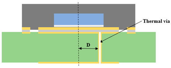
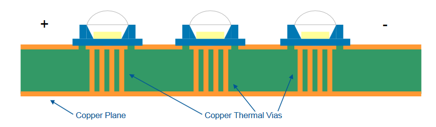
Thermal vias in thick copper PCB designs serve as vertical conduits for heat transfer, bridging surface pads to inner planes or the bottom layer. These vias, typically arrays of small-diameter holes plated with copper, are placed directly under LED thermal pads to maximize contact area. The plating thickness matches the board's heavy copper features, ensuring low thermal resistance. In high-power setups, via tents or fills prevent solder wicking during reflow, maintaining structural integrity.
Array configurations, such as 8 to 16 vias per LED in a grid pattern, balance heat extraction with fabrication yield. Vias draw heat downward, where it spreads via solid copper pours or couples to external sinks. This technique proves essential in compact LED modules where lateral spreading alone suffices not. Design rules specify via diameters from 0.2 to 0.4 mm, with pitches optimized for density without bridging risks.
Proper via placement requires consideration of drill aspect ratios and plating uniformity, especially in thick copper boards. Simulations validate via effectiveness by comparing isothermal lines with and without them. Integrating thermal vias elevates thick copper PCB for LED performance, enabling reliable operation at elevated power levels.
High Power LED PCB Design Best Practices
High power LED PCB design begins with selecting copper weights based on power dissipation and current demands. Engineers allocate solid copper planes under LEDs, extending to board edges for optimal spreading. Trace widths follow conservative margins to accommodate skin effect at high frequencies in dimmable drivers. Multilayer stacks dedicate inner layers to ground pours, interconnected via stitching vias for uniform potential and thermal equipotential.
Component placement prioritizes heat sources centrally or near edges for sink attachment, with spacing to avoid mutual heating. Silkscreen and solder mask openings expose copper for convection enhancement. Thermal reliefs on pads prevent warping during soldering, a critical step in assembly readiness. Validation involves infrared thermography post-prototype to correlate simulations with reality.
Best practices emphasize iterative design, incorporating feedback from manufacturing on etch factors for thick copper features.
Aluminum vs Thick Copper PCBs for LED Applications
Aluminum substrate PCBs, often metal-clad with thin copper circuits, excel in moderate power LED lighting due to their integrated heat spreading core. These boards feature a dielectric layer bonding aluminum to copper foil, typically 1 ounce, prioritizing lightweight construction and cost savings. However, their thermal conductivity relies on the aluminum base, which conducts heat primarily vertically to a sink. Thick copper PCBs on FR4, conversely, leverage heavy outer layers for both lateral and vertical conduction, suiting applications needing high current alongside dissipation.
- Thermal Path: Aluminum PCB — vertical through core; Thick copper PCB — lateral spreading plus vertical vias.
- Current Capacity: Aluminum PCB — moderate, limited by thin copper; Thick copper PCB — high, due to thick traces.
- Weight: Aluminum PCB — lighter; Thick copper PCB — heavier.
- Cost: Aluminum PCB — lower; Thick copper PCB — higher.
- Mechanical Rigidity: Aluminum PCB — good but softer base; Thick copper PCB — excellent rigidity.
- Applications: Aluminum PCB — streetlights, panels; Thick copper PCB — drivers, high-lumen modules.
Thick copper offers superior rigidity for vibration-prone environments like automotive LEDs. Aluminum suits where weight trumps current needs, but thick copper prevails in dense, power-hungry designs. Selection hinges on system-level thermal modeling.
LED PCB Manufacturing Process for Thick Copper
The LED PCB manufacturing process for thick copper demands specialized steps to handle heavy foils without defects. It starts with lamination of thick copper-clad laminates, followed by dry film application for imaging. Exposure and development define circuit patterns, but etching requires differential rates: slower for thick copper to prevent undercuts. Liquid or plasma etching controls sidewall profiles, adhering to IPC-A-600 acceptability criteria.
Post-etch, plating builds via walls to match outer copper thickness, using pulse or DC methods for uniformity. Multilayer pressing employs high-pressure cycles to bond prepregs without voids. Surface finishes like ENIG or HASL protect against oxidation, vital for LED soldering. Final fabrication includes routing, scoring, and electrical testing for continuity and shorts.
Quality controls like cross-section analysis verify copper thickness and plating integrity. These factory-driven processes ensure thick copper boards deliver on thermal promises.
Conclusion
Thick copper PCBs unlock efficient heat dissipation for LED lighting through enhanced conduction and integrated vias. Designers gain actionable strategies for high power LED PCB design, from via arrays to stackup optimization. Comparing with aluminum highlights trade-offs, guiding material choices. Manufacturing precision upholds reliability. Adopting these approaches empowers engineers to build durable, high-performance LED systems.
FAQs
Q1: What role do thermal vias play in thick copper PCB for LED heat management?
A1: Thermal vias transfer heat from LED pads to inner layers or the board bottom in thick copper PCB for LED designs. Arrays of around 0.3 mm vias under pads create low-resistance paths that spread heat effectively, preventing junction overtemperature. Proper factory alignment ensures via plating matches copper weight for optimal thermal performance.
Q2: How does high power LED PCB design incorporate thick copper?
A2: High power LED PCB design uses 2–4 oz copper planes for current and thermal handling. Solid pours connect to thermal via arrays to minimize resistance, while layouts space components for airflow. Simulations and standards guide trace dimensions and thermal margins, sustaining lumen output and reliability under load.
Q3: What are key differences in aluminum vs thick copper PCB for LEDs?
A3: Aluminum PCBs provide a mainly vertical heat path via the metal core and suit lightweight, moderate-current needs. Thick copper PCBs enable strong lateral spreading and high current on FR4 by using heavy copper layers and thermal vias. The choice depends on thermal budget, electrical loading, weight, and mechanical rigidity requirements.
Q4: What challenges arise in the LED PCB manufacturing process for thick copper?
A4: Heavy copper requires controlled etching to avoid undercutting and robust through-hole plating to achieve target wall thickness. Lamination must control warpage from copper imbalances, and finishes like ENIG support reliable soldering. Inspection per IPC standards verifies thickness and integrity, safeguarding thermal and electrical performance without yield loss.
References
IPC-2221B — Generic Standard on Printed Board Design. IPC, 2009
IPC-6012E — Qualification and Performance Specification for Rigid Printed Boards. IPC, 2017
IPC-2152B — Standard for Determining Current Carrying Capacity in Printed Board Design. IPC, 2023
IPC-A-600K — Acceptability of Printed Boards. IPC, 2020


