Introduction
Blind and buried vias represent critical advancements in printed circuit board (PCB) technology, enabling higher component density and shorter signal paths in high-density interconnect (HDI) designs. These vias allow connections between specific layers without penetrating the entire board thickness, which is essential for compact electronics in telecommunications, automotive, and computing applications. However, their manufacturing introduces unique complexities that often result in PCB manufacturing defects, compromising board reliability and performance. Common issues such as via plating issues, drilling inaccuracies, layer misalignment, thermal stress, and challenges in reliability testing demand systematic troubleshooting approaches. Engineers must understand these challenges to ensure production yields and long-term functionality. This article explores the root causes, diagnostic methods, and best practices aligned with industry standards to mitigate these problems effectively.
Understanding Blind and Buried Vias and Their Manufacturing Process
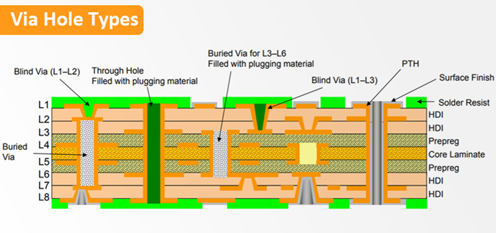
Blind vias connect an outer layer to one or more inner layers without extending through the full board stack-up, while buried vias link only internal layers and remain invisible from the surfaces. These structures are fabricated using sequential lamination processes, where cores with pre-imaged inner layers are built up incrementally with additional prepregs and copper foils. Drilling occurs after partial lamination, often employing laser ablation for microvias or mechanical drilling for larger diameters, followed by desmear, electroless seeding, and electroplating to form conductive barrels. The process requires precise control over layer registration, hole geometry, and plating uniformity to avoid defects. In factory settings, these steps amplify risks compared to through-hole vias due to the limited access for inspection and repair. Adhering to standards like IPC-6012DS for HDI boards ensures minimum performance criteria for via integrity.
The relevance of blind and buried vias stems from the demand for multilayer HDI PCBs in modern electronics, where space constraints drive routing density. Poorly manufactured vias lead to open circuits, signal integrity degradation, or premature failures under operational stresses. Factory-driven insights reveal that yield losses from via-related defects can exceed 20 percent in early production runs without optimized processes. Troubleshooting these elements directly impacts cost, time-to-market, and end-product reliability for electric engineers specifying such boards.
Key Causes of PCB Manufacturing Defects in Blind and Buried Vias
Drilling Inaccuracies
Drilling inaccuracies manifest as off-center holes, breakthrough into unintended layers, or excessive drill wander, particularly challenging for blind vias where depth control is critical. Mechanical drills can deviate due to bit wear, spindle runout, or material inconsistencies, while laser drilling faces issues with ablation rates varying by resin type. These errors stem from inadequate drill entry and exit materials or insufficient fiducial alignment during multi-stage builds. In buried vias, inaccuracies propagate hidden until electrical testing reveals opens. Factory experience shows that tolerances tighter than 50 microns demand advanced tooling and entry board optimization. Such defects directly contribute to layer misalignment if not caught early.
Via Plating Issues
Via plating issues, including voids, seams, and thin copper deposits, arise from poor electroless seed layer adhesion, uneven current distribution in electrolytic plating, or inadequate desmear processes leaving residue. In blind and buried vias, the high aspect ratios exacerbate throwpower limitations, where electrolyte penetration diminishes at hole bottoms. Gas entrapment during plating generates voids that weaken barrel integrity, especially under thermal cycling. Factory plating lines must maintain consistent bath chemistry, agitation, and anode configurations to achieve uniform coverage. IPC-A-600K provides acceptability criteria for plating continuity and thickness, guiding visual and microscopic inspections. Unresolved plating defects often lead to reliability failures in field use.
Layer Misalignment
Layer misalignment occurs during sequential lamination when cores shift relative to outer layers due to differential thermal expansion, pressure variations, or poor optical fiducial registration. Blind vias require exact hole positioning to intersect pads on target inner layers, and even minor offsets cause non-contact opens. Buried vias amplify this risk as multiple inner cores stack without surface references. Contributing factors include prepreg flow inconsistencies or drill-to-photo alignment errors in imaging steps. Engineers observe that symmetric stack-ups and pin lamination reduce shifts, but high-layer-count boards remain prone. This defect interconnects with drilling inaccuracies, compounding overall yield issues.
Thermal Stress Effects
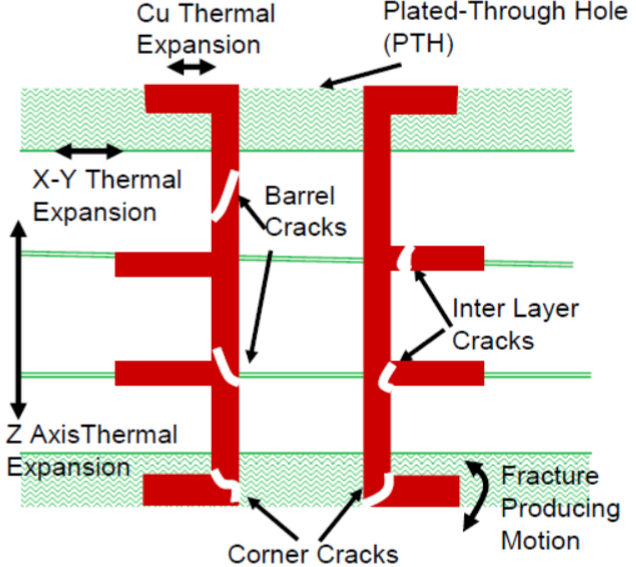
Thermal stress induces cracks, delamination, or barrel separation in vias due to coefficient of thermal expansion (CTE) mismatches between copper plating and dielectric materials during reflow soldering or operational heating. Blind vias, with exposed ends, experience higher stress concentrations at interfaces, while buried vias suffer from enclosed expansion constraints. Repeated thermal excursions propagate micro-cracks initiated by plating voids or thin walls. Factory bake-out and controlled ramp rates mitigate initial stresses, but material selection plays a pivotal role. JEDEC standards outline thermal cycling tests to simulate these conditions, revealing weaknesses early. Thermal stress remains a primary failure mode in reliability testing.
Practical Troubleshooting and Best Practices
Troubleshooting begins with in-process monitoring using automated optical inspection (AOI) for surface features and X-ray laminography for hidden buried vias to detect plating voids or misalignments non-destructively. Cross-sectioning representative samples provides definitive analysis of drill depth, plating thickness, and interface integrity, correlating defects to process parameters. Electrical testing, including flying probe continuity and impedance checks, flags functional issues early. For drilling inaccuracies, verify panel registration with vernier scales and adjust entry/exit materials based on drill data logs. Via plating issues respond to pulse plating techniques and post-plating anneals to relieve hydrogen embrittlement.
Best practices emphasize design-for-manufacturability rules, such as limiting blind via aspect ratios to 1:1 and staggering via locations to minimize lamination stresses. Implement sequential build-up with interim inspections after each lamination cycle, ensuring layer-to-layer alignment exceeds IPC-6012DS tolerances. Thermal stress mitigation involves low-CTE core materials and via fill options like conductive epoxy for high-reliability applications. Reliability testing protocols include thermal shock per IPC-TM-650 methods, monitoring resistance changes over cycles. Factories achieve higher yields by integrating statistical process control (SPC) on key metrics like hole wall roughness and plating uniformity. Collaboration between design and manufacturing teams refines panelization and tooling for consistent results.
Troubleshooting Case Insights from Factory Production
In one production scenario involving 12-layer HDI boards with stacked blind vias, initial yields suffered from 15 percent open failures traced to layer misalignment. Cross-sections revealed 75-micron offsets due to asymmetric stack-up causing prepreg skew during lamination. Adjusting to symmetric cores and adding clearance pins resolved the issue, boosting yields to over 95 percent. Another case highlighted via plating issues in micro-blind vias, where bottom voids caused intermittent continuity. Optimizing desmear with plasma treatment and reducing plating current density eliminated seams, validated by extended thermal cycling. These insights underscore the value of root-cause analysis tools like failure mode and effects analysis (FMEA) tailored to blind and buried via processes. Electric engineers benefit from specifying test coupons on panels for targeted reliability verification.
Conclusion
Troubleshooting challenges in blind and buried via PCB manufacturing requires a multifaceted approach addressing drilling inaccuracies, via plating issues, layer misalignment, thermal stress, and rigorous reliability testing. By leveraging standard-aligned processes and advanced inspection, factories minimize PCB manufacturing defects and enhance board longevity. Key takeaways include precise process controls, design optimizations, and proactive testing to ensure high-density designs perform reliably. Electric engineers should prioritize these practices in specifications to avoid costly rework and field failures. Ultimately, mastering these elements supports the evolution of compact, high-performance electronics.
FAQs
Q1: What are the primary causes of via plating issues in blind and buried via manufacturing?
A1: Via plating issues often stem from poor seed layer adhesion, high aspect ratios limiting electrolyte throwpower, and gas entrapment forming voids. Inadequate desmear leaves residues that hinder uniform copper deposition, while inconsistent bath chemistry exacerbates seams. Factory best practices involve plasma desmear and pulse plating to achieve continuous barrels, as guided by IPC-A-600K acceptability criteria. Early detection via cross-sectioning prevents reliability failures.
Q2: How can drilling inaccuracies be minimized in blind via PCB production?
A2: Drilling inaccuracies arise from bit wander, spindle runout, or depth control errors in sequential builds. Use laser drilling for microvias with optimized fluence and mechanical drills with hardened entry boards for stability. Verify fiducial alignment pre-drill and monitor breakthrough with in-line metrology. These steps align with IPC-6012DS tolerances, reducing defects and improving layer registration.
Q3: What role does thermal stress play in PCB manufacturing defects for buried vias?
A3: Thermal stress causes cracking from CTE mismatches during reflow or cycling, propagating from plating imperfections. Buried vias face enclosed stresses leading to delamination. Mitigate with low-CTE materials, via fills, and controlled ramp rates. Reliability testing per JEDEC thermal cycle standards identifies vulnerabilities early, ensuring long-term integrity in high-density boards.
Q4: Why is reliability testing essential for blind and buried via PCBs?
A4: Reliability testing simulates operational stresses to uncover latent defects like thermal-induced cracks or plating voids. Methods include thermal shock, humidity exposure, and resistance monitoring. It validates via performance under IPC-TM-650 conditions, preventing field failures. For electric engineers, this confirms design margins in HDI applications.
References
IPC-6012DS — Qualification and Performance Specification for High Density Interconnect (HDI) Printed Boards. IPC.
IPC-A-600K — Acceptability of Printed Boards. IPC.
IPC-4761 — Design and Qualification of Printed Circuit Boards and Printed Circuit Board Components for Via Protection. IPC.
JEDEC J-STD-020E — Moisture/Reflow Sensitivity Classification of Nonhermetic Solid State Surface Mount Devices. JEDEC.


