Introduction
Sequential build-up PCB manufacturing represents a critical process for producing high-density interconnect boards essential in modern electronics. Electric engineers rely on these PCBs for compact devices like smartphones, medical equipment, and automotive systems where multilayer complexity demands precise layer stacking. However, the sequential nature of the process, involving repeated cycles of dielectric application, via formation, and metallization, introduces unique troubleshooting challenges. Common issues such as sequential build-up PCB delamination, sequential build-up PCB via failures, sequential build-up PCB warpage, and other sequential build-up PCB manufacturing defects can compromise reliability and yield. Understanding these problems requires a factory-driven perspective aligned with industry standards to ensure robust designs. This guide provides practical insights for engineers to diagnose and mitigate defects effectively.
What Is Sequential Build-Up PCB Manufacturing and Why It Matters
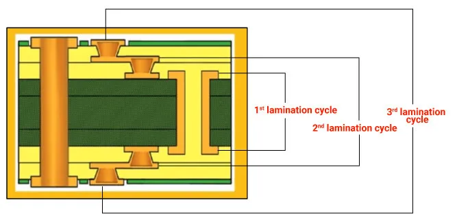
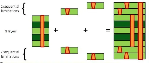
Sequential build-up, often abbreviated as SBU, is a fabrication technique for high-density interconnect PCBs that builds layers incrementally rather than all at once. The process starts with a core substrate, followed by sequential deposition of thin dielectric films, laser drilling for microvias, electroplating of copper, and patterning. Each build-up cycle adds interconnect density, enabling finer pitches and stacked vias critical for advanced applications. For electric engineers, SBU PCBs matter because they support signal integrity in high-speed designs while minimizing board size.
The relevance stems from the growing demand for miniaturization in sectors like telecommunications and computing. Poor process control in SBU leads to higher defect rates compared to standard multilayer builds due to the cumulative effects of multiple cycles. Engineers must grasp these nuances to select appropriate stackups and predict performance under thermal stress. Ultimately, mastering SBU troubleshooting enhances product reliability and reduces costly rework in production.
Common Challenges in Sequential Build-Up PCB Manufacturing
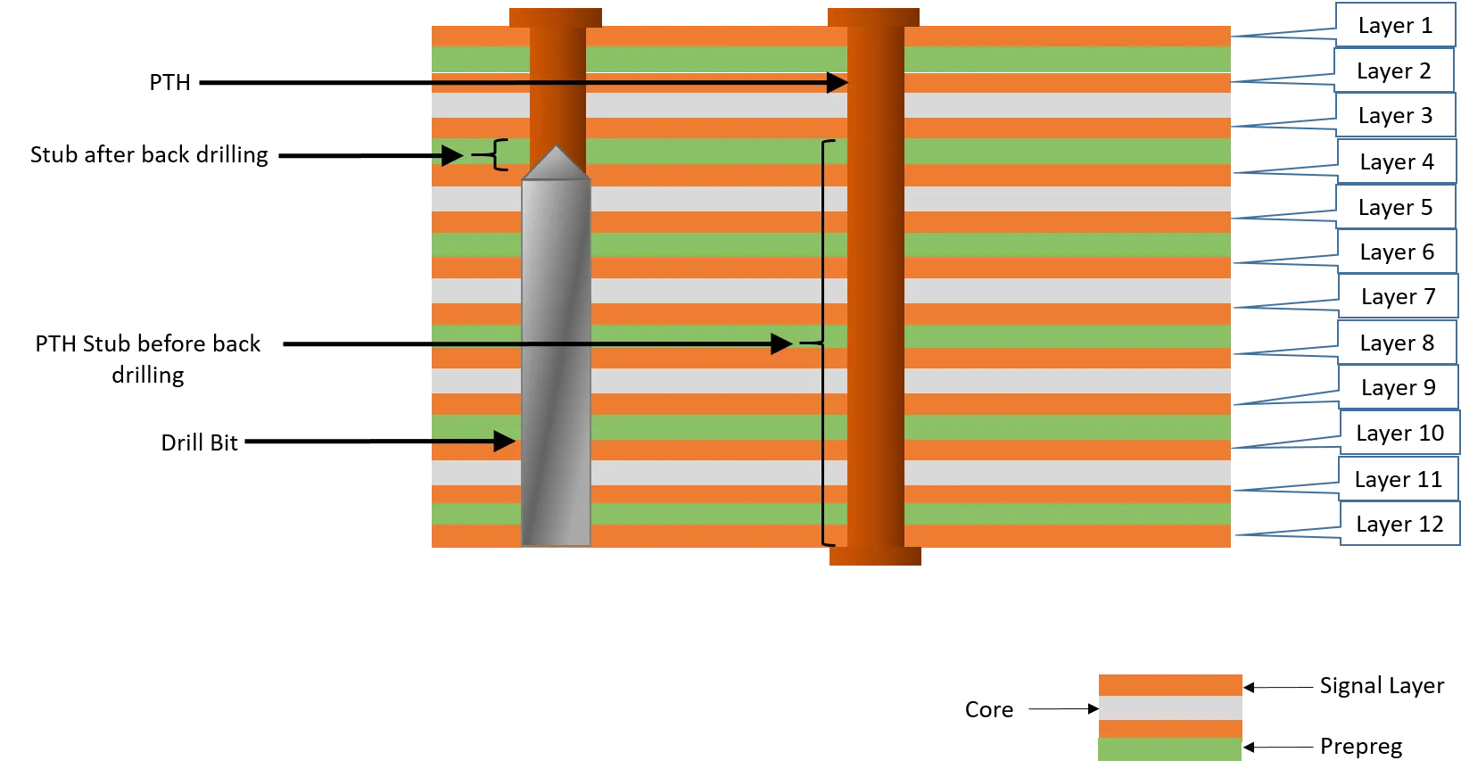
Sequential build-up PCB manufacturing defects manifest in several forms, with delamination being one of the most prevalent. Sequential build-up PCB delamination occurs when dielectric layers separate from copper foils or adjacent layers, often visible as blisters or lifts during inspection. This defect disrupts electrical continuity and mechanical integrity, leading to field failures in harsh environments. Engineers frequently encounter it after lamination or desmear processes where adhesion weakens.
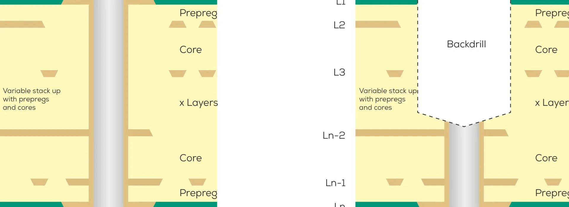
Another critical issue is sequential build-up PCB via failures, which include opens, high resistance, or cracks in microvias. These failures arise from plating voids or barrel cracking under thermal cycling, compromising high-speed signal paths. Warpage represents a third major challenge, where boards bow or twist beyond acceptable limits, complicating assembly and causing misalignment. Sequential build-up PCB warpage exacerbates with asymmetric stackups or mismatched material properties across layers.
Other sequential build-up PCB manufacturing defects include smear residue in vias, plating anomalies, and dielectric cracks. These issues collectively lower yields and increase costs, demanding vigilant process monitoring. Electric engineers must prioritize early detection through inline metrology to maintain quality.
Root Causes and Mechanisms Behind Key Defects
Delamination in sequential build-up PCBs stems primarily from inadequate surface preparation between layers. Contaminants like residues from desmear or insufficient plasma treatment reduce bond strength, allowing moisture ingress during subsequent cycles. Thermal expansion mismatches between dielectrics and copper further propagate stresses, leading to cohesive or adhesive failures at elevated temperatures. The sequential layering amplifies these effects as each cycle introduces potential weak interfaces.
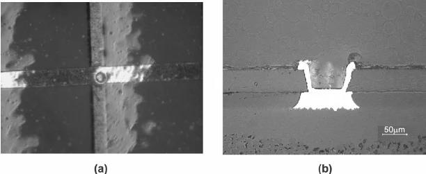
Via failures trace back to drilling inaccuracies and electroless copper seeding inconsistencies. Laser via drilling can cause heat-affected zones that weaken dielectrics, while electroplating defects like dog-boning create stress risers prone to cracking. Under cyclic loading, these vias experience barrel strain exceeding material limits, resulting in opens. Engineers observe this through cross-section analysis revealing voiding or necking.
Warpage mechanisms involve coefficient of thermal expansion (CTE) differentials across the stackup. Core materials with higher CTE than build-up dielectrics induce bowing during cool-down from lamination temperatures. Asymmetric via filling or copper distribution unevenly distributes forces, compounding the issue. Sequential processes heighten sensitivity since early layers influence overall symmetry.
These mechanisms interconnect; for instance, warpage can induce via stresses, accelerating failures. Moisture absorption exacerbates all defects by creating steam pressure during reflow. Factory insights reveal that process variations like resin flow inconsistencies contribute to nonuniform dielectric thickness, amplifying risks.
Practical Troubleshooting Strategies
Effective troubleshooting begins with systematic inspection protocols tailored to SBU characteristics. For sequential build-up PCB delamination, perform C-scan ultrasonics or acoustic microscopy to detect voids noninvasively before final lamination. Cross-sectioning suspect panels at multiple build-up levels confirms failure modes, guiding surface treatment optimizations like enhanced plasma etching. Engineers should correlate defect locations with process logs to isolate cycle-specific issues.
Addressing sequential build-up PCB via failures requires electrical testing via flying probe or bed-of-nails, followed by high-resolution X-ray for barrel integrity. If failures cluster, adjust laser parameters to minimize heat input and improve desmear uniformity. Implement via chain continuity tests after each build-up cycle to catch issues early. Adherence to IPC-A-600 acceptability criteria ensures consistent evaluation.
To combat sequential build-up PCB warpage, measure bow and twist using dial gauges or laser profilometers per IPC-TM-650 methods. Balance stackups by symmetrizing build-up on both sides of the core and selecting low-CTE resins. Controlled cool-down ramps post-lamination minimize residual stresses. Simulate warpage with finite element analysis during design to preempt problems.
Best practices include rigorous material qualification and process DOE. Qualify dielectrics for adhesion per peel strength tests and vias for reliability via thermal cycling. Standardize build-up cycles with automated controls for drilling alignment and plating thickness. J-STD-001 guidelines aid in verifying solderability post-fabrication.
- Delamination — Primary Inspection Method: Acoustic Microscopy — Key Mitigation Step: Plasma Surface Treatment
- Via Failures — Primary Inspection Method: X-ray Cross-Section — Key Mitigation Step: Optimized Laser Drilling
- Warpage — Primary Inspection Method: Profilometry — Key Mitigation Step: Symmetric Stackup Design
- General Defects — Primary Inspection Method: Electrical Testing — Key Mitigation Step: Inline Process Monitoring
Real-World Troubleshooting Insights
In a typical factory scenario, sequential build-up PCB manufacturing defects emerged after scaling production for a high-layer-count design. Initial warpage exceeded limits on outer layers, traced to CTE mismatch via simulation. Adjusting dielectric selection and adding blind via staggering resolved it without yield loss. Sequential build-up PCB delamination appeared in stacked vias, mitigated by refining black hole desmear chemistry.
Another case involved via failures during reliability testing. Cross-sections revealed plating cracks from over-etching; reverting to milder permanganate reduced recurrence. These examples underscore iterative process tuning. Engineers benefit from failure mode analysis to build institutional knowledge.
Conclusion
Troubleshooting sequential build-up PCB manufacturing demands a blend of process understanding and precise diagnostics. By targeting sequential build-up PCB delamination, via failures, warpage, and related defects through root cause analysis, engineers achieve higher yields and reliability. Factory-driven best practices, informed by standards like IPC-A-600 and J-STD-001, form the backbone of success. Proactive measures from design to fab ensure SBU PCBs meet demanding applications. Electric engineers equipped with these strategies can navigate complexities confidently.
FAQs
Q1: What causes sequential build-up PCB delamination most frequently?
A1: Sequential build-up PCB delamination often results from poor interlayer adhesion due to contaminants or inadequate surface activation. Moisture trapped during lamination cycles generates pressure under heat, promoting separation. Engineers mitigate this by standardizing plasma treatments and verifying peel strength. Consistent process controls prevent recurrence across multiple build-ups.
Q2: How do you detect sequential build-up PCB via failures early?
A2: Use continuity testing after each via fill cycle combined with X-ray for void detection. Electrical opens or resistance spikes signal issues like plating defects. Cross-section sampling confirms mechanisms such as barrel cracking. Early intervention preserves yield in high-density designs.
Q3: What are effective ways to reduce sequential build-up PCB warpage?
A3: Balance the stackup symmetrically and match CTE values between core and build-up materials. Implement slow cool-down post-lamination to relieve stresses. Profilometry verifies compliance with allowable bow and twist. Design simulations predict and prevent excessive deformation.
Q4: Can sequential build-up PCB manufacturing defects be fully eliminated?
A4: While not fully eliminable due to process variability, defects like delamination and via failures minimize through DOE and inline monitoring. Standards guide acceptability thresholds. Continuous improvement yields near-perfect panels in mature lines.
References
IPC-A-600K — Acceptability of Printed Boards. IPC, 2020
IPC-TM-650 — Test Methods Manual. IPC, 2018
J-STD-001H — Requirements for Soldered Electrical and Electronic Assemblies. IPC, 2018