Understanding PCB Panelization and Its Importance
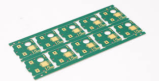
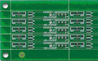
PCB panelization is a crucial manufacturing technique where multiple individual printed circuit boards (PCBs) are grouped together on a larger, single panel. This process is instrumental in enhancing manufacturing efficiency by enabling the simultaneous production and assembly of numerous boards. The advantages are clear: reduced handling time for individual units, lower overall production costs, and a streamlined assembly line. However, if not executed correctly, panelization can introduce a myriad of issues, ranging from significant manufacturing defects to costly production delays.
A well-engineered panelization strategy is the foundation for avoiding these common pitfalls. It ensures that the individual boards maintain their structural integrity throughout the fabrication, assembly, and testing phases. Furthermore, proper panel design significantly simplifies and safeguards the depaneling process—the critical step of separating individual PCBs from the larger panel after assembly. This guide will delve into the most frequently encountered panelization challenges and provide actionable solutions to overcome them.
Common Issues in PCB Panelization and Their Underlying Causes
Problems associated with PCB panelization can manifest at various stages of the manufacturing lifecycle. Below, we examine the most prevalent issues, including PCB panel warp, depaneling difficulties, component misalignment, and other manufacturing defects, alongside their primary causes.
PCB Panel Warp
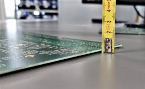
PCB panel warp refers to the undesirable bending, twisting, or bowing of the panel either during or after the manufacturing process. This distortion can severely complicate subsequent assembly steps and even cause damage to sensitive components or traces. Common contributors to warping include:
● Uneven Material Distribution: An imbalance in the distribution of copper layers or substrate materials across the panel can lead to differential thermal expansion during high-temperature processes like soldering. This uneven stress often results in significant panel deformation.
● Suboptimal Panel Design: Large panels that lack adequate structural support or feature poorly positioned breakaway tabs are prone to bending under their own weight or during routine handling throughout the production line.
● Thermal Stress: Exposure to extreme temperatures, particularly during lead-free reflow soldering processes where temperatures can exceed 260°C, causes materials to expand and contract. If this occurs unevenly, it induces internal stresses that lead to warping.
PCB Depaneling Difficulties
Depaneling is the process of precisely separating individual PCBs from the assembled panel. Challenges during this stage, such as cracked boards or damaged components, typically originate from:
● Flawed Scoring or Routing Design: If V-grooves (partial cuts) or mouse bites (perforated tabs) are not designed with appropriate depth, width, or spacing, boards may not separate cleanly. For instance, a V-groove depth less than 30% of the board thickness can induce excessive stress, leading to breakage or splintering during separation.
● Inadequate Tooling: The use of worn, dull, or incorrect depaneling tools can result in rough, jagged edges, or introduce microcracks within the board material, compromising its structural integrity.
● Component Proximity: Components positioned too close to the panel edges (sometimes less than 5mm) are highly vulnerable to mechanical stress and damage during the depaneling operation.
PCB Panel Component Misalignment
Inaccurate placement of components on a panelized PCB during SMD PCB assembly can lead to critical soldering defects, rendering boards non-functional. Key reasons for component misalignment include:
● Imprecise Fiducial Marks: Fiducial marks are optical reference points essential for automated pick-and-place machines to accurately align components. If these marks are incorrectly placed, obscured, or poorly defined, even minute errors (as small as 0.1mm) can cause significant component misplacement.
● Panel Flexing: Any warping or flexing of the panel during the automated assembly process can cause components to shift from their intended positions before or during soldering, leading to incorrect placement.
● Machine Calibration Errors: Automated assembly equipment requires precise calibration to account for specific panel dimensions and manufacturing tolerances. Calibration inaccuracies can result in consistent component placement errors across the entire panel.
Other PCB Panel Manufacturing Defects
Beyond warp and misalignment, various other manufacturing defects can impact PCB panels, including delamination (separation of layers), broken traces, or incomplete etching. These problems are often a consequence of:
● Substandard Material Quality: The use of low-quality substrates or laminates can lead to weak adhesion between layers, making the panel susceptible to delamination under thermal or mechanical stress.
● Improper Handling: Rough or careless handling of panels during the fabrication or assembly stages can cause physical damage such as cracks, scratches, or even broken traces.
● Design Flaws: Inadequate spacing between individual boards on the panel or insufficient edge clearance (e.g., less than 2mm) can result in errors during automated cutting, drilling, or routing operations, leading to damaged boards.
Effective Solutions for Common PCB Panelization Problems
Identifying the root causes of panelization issues is the first step; implementing targeted solutions is the next. Here are actionable strategies to troubleshoot and prevent common PCB panelization problems, ensuring high-quality and reliable manufacturing outcomes.
Resolving PCB Panel Warp
To mitigate or entirely prevent PCB panel warp, consider these strategic approaches:
● Achieve Balanced Copper Distribution: Design the PCB with an even distribution of copper across all layers. Utilize design software to analyze copper density and, if necessary, adjust trace layouts or incorporate dummy copper fills to achieve a balance within 10% across layers. This minimizes differential thermal expansion.
● Incorporate Structural Support: For larger panels, integrate breakaway rails or additional support tabs along the edges. A rail width of 5-10mm can significantly enhance rigidity and prevent bending during processing and handling.
● Optimize Thermal Profiles: Fine-tune reflow soldering profiles to reduce thermal stress. For lead-free soldering, limit peak temperatures to 245-260°C and ensure a gradual cooling phase. This controlled cooling prevents abrupt material contraction and reduces warping tendencies.
Addressing PCB Depaneling Challenges
Preventing issues during the depaneling phase requires meticulous planning in both the design and execution stages:
● Precision in V-Groove and Mouse Bite Design: When using V-grooves, design them with a depth of 30-40% of the board thickness and a width of approximately 0.3mm to ensure clean, stress-free separation. For mouse bites, use a hole diameter between 0.8-1.2mm, with 5-7 holes evenly spaced along the intended break line for optimal performance.
● Utilize Appropriate Depaneling Tools: Invest in high-quality, precision depaneling equipment such as specialized routers or laser cutters. These tools ensure clean cuts, minimizing mechanical stress on the boards and preventing jagged edges or microcracks.
● Protect Vulnerable Components: Maintain a minimum clearance of 5mm between any component and the panel edges. This critical buffer zone helps protect components from mechanical damage during the depaneling process. If space is extremely limited, consider using temporary protective tape or custom fixtures during depaneling.
Correcting PCB Panel Component Misalignment
Ensuring the accurate placement of components on panelized PCBs involves careful setup and attention to detail:
● Verify Fiducial Marks: Implement at least three fiducial marks on the panel, ideally located near the corners, with a diameter of 1-2mm. These marks should have clear contrast against the PCB background. Critically, double-check their precise positions in the design files before proceeding to fabrication.
● Minimize Panel Flexing: Utilize rigid PCB materials for the panel and ensure robust clamping mechanisms are in place during the assembly process to prevent any unwanted movement or flexing. A panel thickness of at least 1.6mm is generally recommended for most applications to enhance stability.
● Regular Equipment Calibration: Implement a strict schedule for regularly calibrating pick-and-place machines to maintain placement accuracy, ideally within 0.05mm. Conduct thorough test runs on sample panels to confirm precise component alignment before initiating full-scale production.
Preventing Other PCB Panel Manufacturing Defects
Minimizing various manufacturing defects begins with stringent quality control and thoughtful design practices:
● Select Premium Materials: Choose high-quality, reliable substrates and laminates with consistent physical and chemical properties. For instance, PCB FR-4 material with a glass transition temperature (Tg) of 130-140°C is a robust choice for most standard applications, offering good thermal stability.
● Adhere to Design Guidelines: Maintain a minimum edge clearance of 2-3mm between individual boards on the panel. This provides a necessary buffer to prevent cutting or drilling errors during fabrication. Additionally, include clear markings for panel orientation to avoid handling mistakes during manual or automated processes.
● Implement Robust Quality Checks: Integrate visual inspections and Automated Optical Inspection (AOI) systems after each critical manufacturing stage. AOI, for example, can detect defects such as trace breaks or misaligned vias with an accuracy often exceeding 99.9%, allowing for early identification and rectification of issues.
Best Practices for Successful PCB Panelization
Beyond addressing specific issues, adopting comprehensive best practices for PCB panelization can significantly optimize your manufacturing processes, saving valuable time and resources in the long term.
● Early Collaboration with Manufacturers: Initiate communication with your fabrication and assembly partners during the early design and planning phases. Share your panelization design files. Their expert feedback on aspects like optimal panel size, placement of tooling holes, and other crucial specifications can preemptively resolve potential manufacturing issues.
● Adhere to Standard Panel Sizes: Whenever feasible, utilize industry-standard panel dimensions (e.g., 18x24 inches or 9x12 inches). This compatibility with standard manufacturing equipment helps reduce setup times and associated costs, improving overall efficiency.
● Conduct Pre-Production Testing: Before committing to a full production run, always produce a small batch of panels for comprehensive testing. This pilot run allows for the early identification of potential problems such as PCB panel warp or component misalignment, mitigating the risk associated with a large-scale order.
● Maintain Detailed Documentation: Keep meticulous records of all your panelization designs. This documentation should include critical details like tab placements, V-groove or mouse bite specifications, and chosen material types. Such records are invaluable for troubleshooting any recurring issues and continuously improving future designs.
Choosing the Optimal Panelization Method
The selection of the appropriate panelization method is crucial, as each technique is best suited for different project requirements and can help avoid specific PCB panelization problems.
● Tab Routing with Breakaway Tabs: In this method, individual boards are held together by small tabs that are manually or mechanically broken off after assembly. It is particularly effective for small to medium-sized boards and designs with irregular shapes. However, careful placement of tabs is necessary to prevent stress points that could damage the board during separation.
● V-Groove Scoring: This technique involves cutting V-shaped grooves into the top and bottom surfaces of the panel, creating weakened lines for easy separation. V-groove scoring is highly effective for rectangular boards and can minimize damage during depaneling, provided the grooves are designed with the correct depth and angle.
● Mouse Bites: This method utilizes small, perforated holes to connect boards within the panel, allowing for manual separation by snapping. Mouse bites are often cost-effective for low-volume production or when curved separation lines are required. However, they may not be ideal for delicate or high-density boards, as the snapping process can introduce minor stress or leave small "nibs" along the edge.
Conclusion: Mastering PCB Panelization for Enhanced Manufacturing Outcomes
PCB panelization is an indispensable stage in the electronics manufacturing process, yet it frequently presents challenges such as PCB panel warp, difficulties during depaneling, and component misalignment. By thoroughly understanding the root causes of these prevalent PCB panelization problems and diligently implementing the solutions and best practices detailed in this guide, manufacturers can achieve substantial improvements in both the quality and efficiency of their production runs.
Every detail in the panelization process, from meticulously balancing copper distribution and optimizing V-groove designs to ensuring the precise placement of fiducial marks, plays a critical role. Dedicating the necessary time to carefully design and rigorously test your panels will be instrumental in circumventing costly production delays and consistently producing reliable, high-performance PCBs. Armed with these comprehensive strategies, you are now well-equipped to address and mitigate any PCB panel manufacturing defects, thereby significantly streamlining your entire workflow.
Begin integrating these practical tips into your forthcoming projects to observe a noticeable positive impact on your results. It is important to remember that proactive preparation is a powerful tool, ensuring a seamless and efficient panelization and assembly process from start to finish.


