Introduction
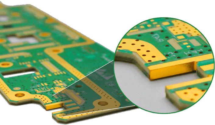
Via filling plays a critical role in modern printed circuit board manufacturing, particularly for high-density interconnect boards and applications requiring reliable power and signal integrity. Filled vias eliminate air gaps, enhance thermal management, and support via-in-pad designs that shorten signal paths. However, defects such as via filling voids, uneven copper plating, and barrel stress in filled vias can compromise board reliability, leading to failures in electrical continuity and mechanical integrity. These PCB manufacturing defects demand systematic troubleshooting to maintain performance under thermal and mechanical stresses. Electric engineers must understand the root causes and resolution strategies to ensure compliance with industry standards and optimize production yields. This article explores identification methods, failure analysis techniques, and practical solutions drawn from factory processes.
Understanding Via Filling and Its Importance
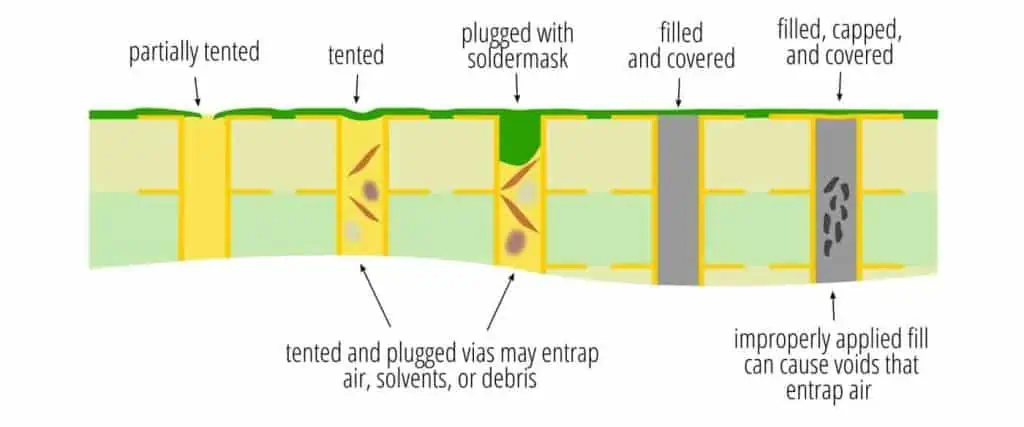
Via filling involves depositing conductive or non-conductive materials into drilled vias to achieve complete barrel coverage, often followed by capping for planar surfaces in high-reliability applications. In PCB manufacturing, this process supports stacked microvias in HDI boards and prevents solder wicking during assembly. Without proper filling, vias remain susceptible to environmental factors like moisture ingress and thermal expansion mismatches. The relevance intensifies in electric engineering contexts, where filled vias handle high currents or high-speed signals without impedance discontinuities. Defects like via filling voids reduce cross-sectional area, increasing resistance and heat generation. Adhering to standards such as IPC-4761 ensures via protection types, from tenting to fully filled structures, meet performance needs.
Factory-driven insights reveal that via filling enhances structural stability, especially under cyclic thermal loads common in power electronics. Poorly filled vias contribute to PCB manufacturing defects that manifest as intermittent failures post-assembly. Engineers benefit from recognizing how filling techniques align with board class requirements, such as those in IPC-6012 for qualification.
Common Via Filling Defects
Via Filling Voids
Via filling voids appear as gaps or air pockets within the via barrel, ranging from small spherical inclusions to large irregular cavities. These defects weaken electrical conductivity and mechanical strength, potentially leading to open circuits under stress. In cross-sections, voids often cluster near the via center due to plating dynamics. Large voids exceed acceptable limits, accelerating fatigue in high-reliability boards. Factory inspections frequently detect them via X-ray or microscopy during quality control.
Uneven Copper Plating
Uneven copper plating manifests as variations in thickness along the via walls, with thin spots prone to cracking and thick areas causing protrusions. This defect arises from inconsistent current distribution during electroplating, resulting in high-resistance paths. In filled vias, uneven plating exacerbates void formation by trapping gases. Visual and electrical testing reveals hotspots or dimples on the surface. Such inconsistencies violate uniformity requirements in manufacturing processes.
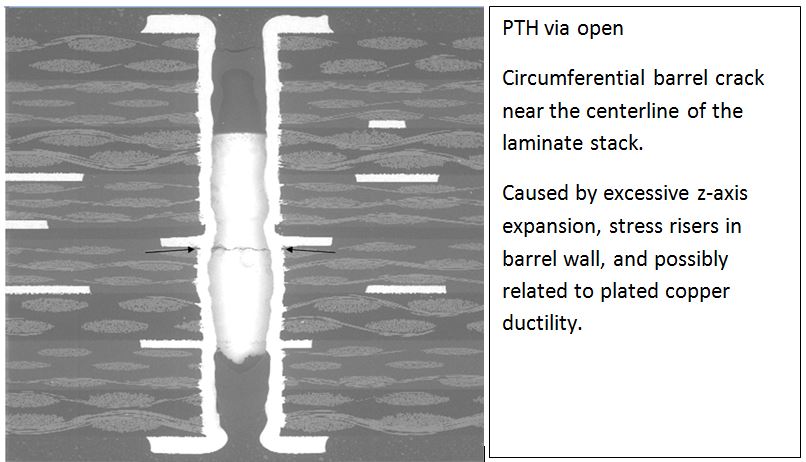
Barrel Stress in Filled Vias
Barrel stress in filled vias causes cracking in the copper lining, often near the midplane where tensile forces peak during thermal cycling. Coefficient of thermal expansion (CTE) mismatches between the fill material, copper, and dielectric generate these stresses. Cracks propagate under repeated reflow or operation, leading to electrical discontinuity. Failure analysis confirms fractures via cross-sectioning, highlighting delamination risks. This defect underscores the need for material compatibility in design.
Root Causes of Via Filling Defects
Contamination from drilling debris or airborne particles disrupts uniform deposition, fostering via filling voids during resin or copper filling. Air bubbles trapped in hole sides, often from high surface tension solvents in cleaning, prevent complete wetting and create pockets. Rough hole walls from improper drill parameters, such as excessive speeds, lead to uneven adhesion and plating inconsistencies.
Imbalanced plating baths with incorrect chemical proportions or inadequate agitation cause uneven copper plating, as ions deplete faster near entrances. Environmental impurities, including microparticles from equipment, embed in the barrel and nucleate voids. For barrel stress, thin copper plating below recommended thicknesses fails to withstand CTE-induced strains, while mismatched fill materials amplify shear forces.
High aspect ratios complicate electrolyte flow, promoting stagnant zones and defects. Factory data links these to process variations, like insufficient desmearing, which leaves resin smears blocking plating.
Failure Analysis of Filled Vias
Failure analysis of filled vias begins with non-destructive methods like X-ray imaging to detect voids exceeding 5% of barrel volume or incomplete fills. Electrical testing, such as continuity checks under thermal cycling, identifies intermittent opens from barrel stress. Cross-sectioning at suspect locations reveals void morphology, plating thickness, and crack propagation.
Scanning electron microscopy (SEM) quantifies copper grain structure and adhesion interfaces, pinpointing contamination origins. Dye penetrant testing highlights microcracks invisible to optical inspection. Per IPC-A-600, cap plating analysis assesses planarity, voids, and separations between cap and fill. Engineers correlate findings to process steps, such as plating or filling, for root cause isolation.
Layered analysis in HDI boards may require sequential polishing to expose stacked vias. Documentation of defect size, location, and board class guides corrective actions.
Troubleshooting and Resolution Strategies
Address via filling voids by selecting low surface tension solvents for cleaning and implementing vacuum-assisted filling to expel air. Enclose plating lines to minimize impurities, and filter electrolytes regularly to remove particulates. Pulse reverse plating improves uniformity over direct current, reducing uneven copper plating by enhancing mass transport.
For barrel stress in filled vias, specify thicker copper plating, targeting at least 25 microns, and select fill materials with CTE matched to the dielectric. Optimize desmearing to smooth walls, preventing rough surfaces that initiate cracks. IPC-6012 guidelines mandate 75% minimum fill for through-hole leads in Class 2 boards, with no voids in Class 3.
Cap plating per IPC-A-600 requires no voids over resin fill and planarity within tolerances, achieved via secondary electroplating and planarization. Monitor bath chemistry with frequent titrations and agitation controls.
- Via Filling Voids — Primary Cause: Air entrapment, contamination; Key Resolution: Vacuum filling, filtered baths
- Uneven Copper Plating — Primary Cause: Poor agitation, chemical imbalance; Key Resolution: Pulse plating, solution checks
- Barrel Stress — Primary Cause: CTE mismatch, thin plating; Key Resolution: Material matching, thicker Cu
Best Practices in PCB Manufacturing
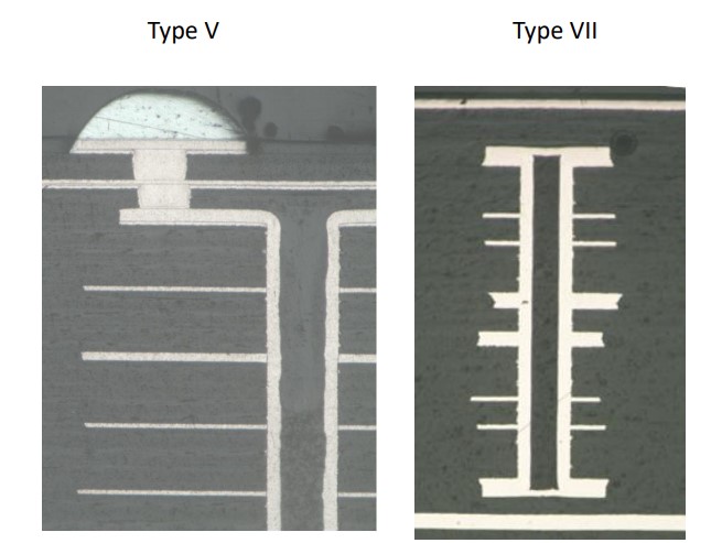
Integrate IPC-4761 via types early in design, selecting Type V for filled non-conductive vias or Type VII for capped structures in via-in-pad applications. Conduct pilot runs to validate process windows for aspect ratios below 10:1. Implement automated optical inspection (AOI) post-plating and filling to catch defects early.
Routine maintenance of drilling and plating equipment ensures consistent hole quality. Collaborate with material suppliers for low-shrinkage fills compatible with low-CTE laminates. Thermal shock testing simulates field conditions, verifying reliability before volume production.
Track yield metrics tied to defect rates, adjusting parameters iteratively.
Conclusion
Troubleshooting via filling defects requires a factory-oriented approach, focusing on process controls to mitigate via filling voids, uneven copper plating, barrel stress in filled vias, and related PCB manufacturing defects. Failure analysis techniques like cross-sectioning and SEM provide actionable insights, while adherence to IPC standards ensures compliance. By optimizing cleaning, plating, and filling steps, engineers achieve robust vias for demanding electric applications. Proactive design and monitoring yield higher reliability, reducing field failures. Implementing these strategies elevates PCB quality across production scales.
FAQs
Q1: What causes via filling voids in PCB manufacturing?
A1: Via filling voids stem from trapped air during cleaning, contamination from particulates, or imbalanced plating baths with poor agitation. High surface tension solvents exacerbate air entrapment, while rough drilling leaves residues that nucleate gaps. Factory solutions include vacuum-assisted filling and filtered electrolytes to achieve complete barrel coverage per IPC-6012 guidelines.
Q3: How do you identify barrel stress in filled vias during failure analysis?
A3: Barrel stress appears as cracks in the copper lining, often mid-barrel, confirmed via cross-section polishing and SEM imaging. X-ray detects density variations from fractures, while thermal cycling tests provoke opens. CTE mismatches between fill and dielectric drive this defect, resolvable by thicker plating and material selection.
Q4: What are the best practices to prevent uneven copper plating in vias?
A4: Prevent uneven copper plating with pulse reverse electroplating for uniform ion distribution and regular bath chemistry checks. Proper desmearing smooths walls for adhesion, and adequate agitation avoids boundary layer stagnation. Target minimum thicknesses align with IPC standards for reliable performance.
Q5: How does IPC-A-600 address cap plating on filled vias?
A5: IPC-A-600 specifies planar copper caps with no voids over resin fill for all classes. Acceptable conditions allow minor separations between cap and fill but prohibit cap-to-plating delamination. Dimples or bumps must meet IPC-6012 dimensional limits, ensuring assembly readiness.
References
IPC-6012E — Qualification and Performance Specification for Rigid Printed Boards. IPC, 2017
IPC-A-600K — Acceptability of Printed Boards. IPC, 2020
IPC-4761 — Design Guide for Protection of Printed Board Via Structures. IPC, 2007