Introduction
Printed Circuit Board assembly errors can disrupt production schedules, increase costs, and compromise the reliability of electronic devices. For electrical engineers, identifying and resolving issues such as Gerber file defects, centroid file errors, solder paste stencil file issues, and CAD file conversion problems is critical to ensuring a seamless manufacturing process. These errors often stem from data inconsistencies, miscommunication between design and assembly teams, or improper file handling. This article dives into the root causes of common PCB assembly errors, their impact on production, and practical solutions to mitigate them. By adhering to industry standards and implementing best practices, engineers can minimize defects and improve assembly outcomes. Whether you are designing complex multilayer boards or troubleshooting assembly line issues, understanding these errors is essential for maintaining quality and efficiency.
What Are PCB Assembly Errors and Why They Matter
PCB assembly errors refer to mistakes or defects that occur during the process of mounting components onto a printed circuit board. These errors can manifest as misplaced components, soldering defects, or complete assembly failures, often leading to nonfunctional products. They matter because even a single error can result in costly rework, delayed product launches, or field failures that damage a project's reputation. For electrical engineers, addressing PCB assembly errors is not just about fixing immediate issues but also about ensuring long term reliability and performance. With the increasing complexity of electronic designs, the risk of errors related to Gerber file defects, centroid file errors, and solder paste stencil file issues grows. Ignoring these problems can lead to significant financial losses and compromised device safety, making error prevention a top priority in the industry.
Causes of PCB Assembly Errors
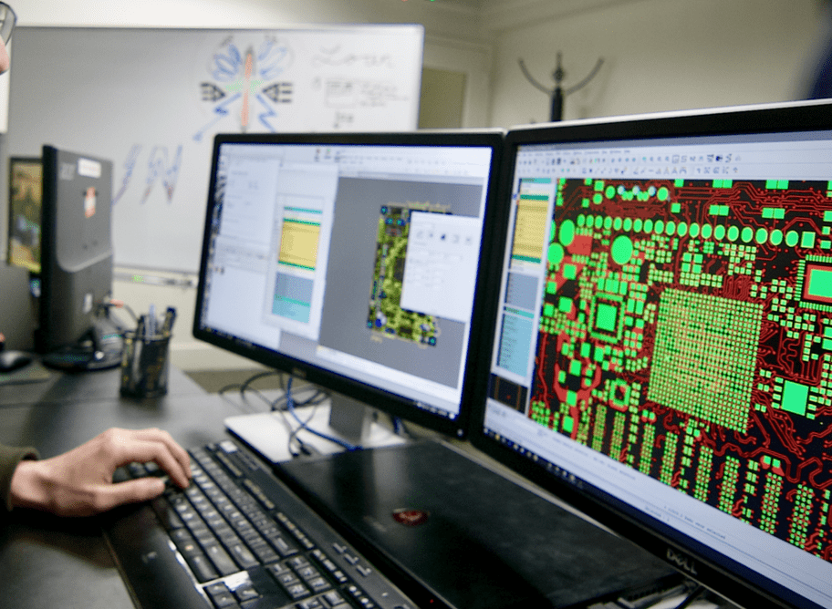
Gerber File Defects
Gerber files serve as the blueprint for PCB fabrication, containing critical information about copper layers, drill holes, and component outlines. Defects in these files can lead to manufacturing errors such as incorrect board dimensions or misaligned layers. Common causes include incomplete data export from design software, version mismatches, or improper file formatting. For instance, missing aperture definitions can result in incorrect trace widths, while unclosed contours may cause fabrication tools to misinterpret shapes. Such issues often cascade into assembly errors, as inaccurate boards cannot accommodate components correctly. Electrical engineers must validate Gerber files against design intent before submission to avoid these costly mistakes.
Centroid File Errors
Centroid files, also known as pick and place files, provide coordinates and orientation data for automated component placement during assembly. Errors in these files can cause components to be placed incorrectly or omitted entirely. Typical issues arise from mismatched component libraries, incorrect rotation values, or missing reference designators. If the centroid data does not align with the physical board layout, assembly machines may misinterpret component positions, leading to functional failures. These errors are particularly problematic in high density designs where precision is paramount. Engineers need to ensure that centroid files are generated accurately and cross checked with the PCB layout.
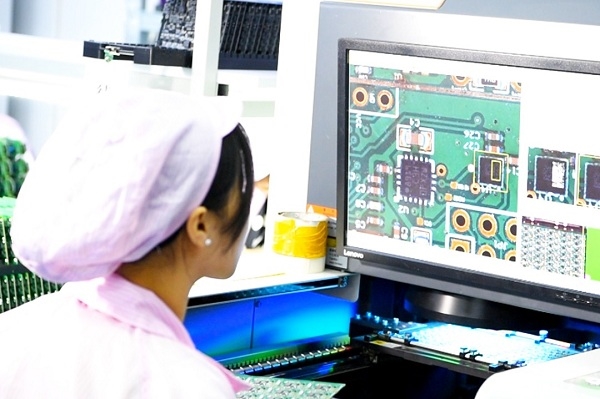
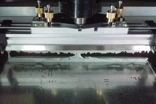
Solder Paste Stencil File Issues
Solder paste stencil files define the pattern for applying solder paste to pads before component placement. Issues in these files, such as incorrect aperture sizes or misaligned patterns, can result in insufficient or excessive solder paste, leading to poor solder joints or bridging. Causes often include improper scaling during file generation or failure to account for board shrinkage during fabrication. These defects directly impact the quality of soldering, a critical step in PCB assembly. For engineers, verifying stencil file accuracy against the board design and fabrication tolerances is essential to prevent soldering defects during production.
Related Reading: How Does Stencil Design Impact PCB Assembly Quality?
CAD File Conversion Problems
CAD file conversion errors occur when design data is translated between different software formats or versions, often leading to data loss or misinterpretation. For example, layer mapping issues during conversion can result in missing traces or incorrect component placements. These problems are common when files are exported for manufacturing without proper validation. Inaccurate conversions can propagate errors into Gerber files, centroid data, and stencil designs, compounding issues during assembly. Electrical engineers must use standardized export protocols and verify converted files to ensure data integrity throughout the design to assembly workflow.
Impact of PCB Assembly Errors on Production
PCB assembly errors can halt production lines, requiring time consuming rework or complete board redesigns. Misplaced components due to centroid file errors may lead to short circuits or open connections, rendering the board unusable. Similarly, solder paste stencil file issues can cause weak solder joints, increasing the risk of failures during testing or operation. Gerber file defects often result in boards that do not match design specifications, leading to assembly mismatches. Beyond immediate production delays, these errors can affect product reliability, especially in critical applications like medical or automotive electronics. Addressing these issues early through rigorous file validation and adherence to industry standards is vital for minimizing disruptions and maintaining quality.
Related Reading: Troubleshooting Common Manufacturing Challenges with Rogers PCBs
Practical Solutions to Mitigate PCB Assembly Errors
Validating Gerber Files
To prevent Gerber file defects, engineers should use design rule checks before file generation to ensure all layers are correctly defined. Cross verifying the output files against the original design helps identify discrepancies in traces or drill holes. Additionally, adhering to guidelines outlined in standards such as IPC-2581 for digital product model exchange can streamline data accuracy. Regular updates to design software also reduce the risk of export errors. Implementing these steps ensures that fabrication proceeds without misinterpretation of critical design elements.
Ensuring Centroid File Accuracy
Centroid file errors can be minimized by synchronizing component libraries with the PCB layout during file generation. Engineers should verify that reference designators match between the schematic and layout, and double check rotation values for each component. Automated tools for pick and place data validation can flag inconsistencies before assembly begins. Following best practices ensures that automated machines place components precisely, reducing the likelihood of misplaced parts during production.
Optimizing Solder Paste Stencil Files
For solder paste stencil file issues, engineers must confirm that aperture dimensions match pad sizes on the PCB layout. Accounting for fabrication tolerances and potential board shrinkage during design prevents misalignment. Standards like IPC-7525B, which provides guidelines for stencil design, can be referenced to ensure optimal solder paste application. Reviewing stencil files alongside Gerber data also helps catch scaling errors before manufacturing. These measures contribute to consistent soldering quality across production runs.
Streamlining CAD File Conversion
To address CAD file conversion problems, engineers should use standardized file formats for data exchange between design and manufacturing stages. Validating converted files against the original design ensures that no data is lost or altered. Maintaining consistent software versions across teams reduces compatibility issues. Adhering to protocols outlined in standards such as IPC-2610 for documentation can further minimize conversion errors. These practices preserve design intent throughout the assembly process.
Troubleshooting Common PCB Assembly Errors
When PCB assembly errors occur, a systematic troubleshooting approach is necessary. Start by reviewing Gerber files for fabrication related defects if the board dimensions or layers appear incorrect. For component placement issues, inspect the centroid file for inaccurate coordinates or orientation data. Soldering defects often point to solder paste stencil file issues, requiring a check of aperture patterns and paste volume. If errors persist, examine CAD file conversion logs for data loss or layer mismatches. Documenting each error and resolution step helps build a knowledge base for future projects. Referencing standards like IPC-A-610H for acceptability criteria during inspection ensures that troubleshooting aligns with industry expectations.
Best Practices for Preventing PCB Assembly Errors
Preventing PCB assembly errors requires a proactive approach. Begin with comprehensive design reviews to catch potential issues early. Use automated validation tools for Gerber, centroid, and stencil files to ensure data accuracy. Maintain clear communication between design and assembly teams to avoid misinterpretations. Adhere to relevant industry standards, such as IPC-J-STD-001H for soldering requirements, to guide assembly processes. Regularly train team members on file handling and error prevention techniques. Implementing these best practices reduces the risk of errors and enhances overall production reliability.
Conclusion
PCB assembly errors, including Gerber file defects, centroid file errors, solder paste stencil file issues, and CAD file conversion problems, pose significant challenges for electrical engineers. These errors can disrupt production, increase costs, and affect product reliability if not addressed promptly. By understanding their causes, such as data inconsistencies or improper file handling, engineers can implement practical solutions like file validation and adherence to industry standards. A proactive approach, combined with systematic troubleshooting and best practices, ensures smoother assembly processes and high quality outcomes. Prioritizing error prevention ultimately saves time and resources while maintaining the integrity of electronic designs.
FAQs
Q1: What are the most common causes of PCB assembly errors?
A1: PCB assembly errors often stem from Gerber file defects, centroid file errors, and solder paste stencil file issues. Incorrect data export, mismatched component libraries, and improper stencil scaling are frequent culprits. These issues lead to misaligned layers, misplaced components, or poor soldering. Validating files against design intent and following industry standards can significantly reduce such errors during production.
Q2: How can Gerber file defects impact PCB assembly?
A2: Gerber file defects can cause incorrect board dimensions or misaligned layers, leading to assembly mismatches. Components may not fit properly on flawed boards, resulting in placement errors or soldering failures. This disrupts production and requires rework. Engineers should validate Gerber files before fabrication to ensure accuracy and prevent cascading issues in the assembly process.
Q3: What steps can prevent centroid file errors in PCB assembly?
A3: Preventing centroid file errors involves synchronizing component libraries with the PCB layout and verifying reference designators. Double checking rotation values and using automated validation tools also helps. Accurate centroid data ensures precise component placement by assembly machines. Consistent file checks before production minimize the risk of misplaced or omitted components.
Q4: How do solder paste stencil file issues affect soldering quality?
A4: Solder paste stencil file issues, like incorrect aperture sizes or misalignment, lead to uneven solder paste application. This causes weak joints or bridging between pads, compromising soldering quality. Such defects can result in electrical failures during testing. Reviewing stencil files against board design and adhering to relevant standards ensures proper paste deposition for reliable soldering.
References
IPC-2581 - Generic Requirements for Printed Board Assembly Products Manufacturing Description Data and Transfer Methodology. IPC, 2021.
IPC-7525B - Stencil Design Guidelines. IPC, 2012.
IPC-A-610H - Acceptability of Electronic Assemblies. IPC, 2020.
IPC-J-STD-001H - Requirements for Soldered Electrical and Electronic Assemblies. IPC, 2020.
IPC-2610 - Sectional Requirements for Electronic Diagramming Documentation. IPC, 2010.


