What Role Does Solder Mask Play in Printed Circuit Board Functionality?
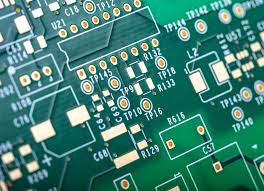
If you're delving into the world of PCB design and manufacturing, a fundamental question often arises: "What exactly is a solder mask, and why is it so crucial?" A solder mask is essentially a thin, protective polymer layer meticulously applied to a printed circuit board (PCB). Its primary function is to encapsulate the copper traces, thereby preventing oxidation and guarding against inadvertent solder bridges during the assembly process. This protective coating is indispensable for guaranteeing the long-term reliability and optimal functionality of your PCB, as it shields the board from environmental factors and precisely directs solder to its designated points. This guide will explore the essential aspects of solder masks, including their necessity, the various types available, popular color choices, and the manufacturing processes involved, providing a foundational understanding of this critical PCB component.
A solder mask, also referred to as solder resist or solder stop, constitutes a polymer layer strategically applied to the surface of a PCB. This delicate coating meticulously covers the copper traces and pads, leaving only those specific areas intended for soldering exposed. It functions as a resilient protective barrier for your circuit board, shielding it from environmental damage, such as oxidation, and ensuring that solder adheres exclusively to the intended contact points during the intricate assembly of PCB process. Without the application of a solder mask, the exposed copper on a PCB would be susceptible to corrosion over time due to continuous exposure to air and moisture. Furthermore, during soldering operations—especially in automated processes like reflow or wave soldering—there is a significant risk that solder could inadvertently connect two adjacent pads, resulting in a short circuit, commonly known as a solder bridge. The solder mask acts as an effective insulator and physical barrier, actively preventing such occurrences. Consequently, it has become an indispensable feature for the vast majority of contemporary PCBs, particularly those produced in high volumes.
Why Is a Solder Mask Indispensable for Modern PCB Manufacturing?
Incorporating a solder mask into your PCB design offers a multitude of critical benefits, rendering it an essential element in the manufacturing process. Let's examine the primary reasons for its widespread adoption.
Shielding Against Oxidation
Copper traces, which form the conductive pathways on a PCB, are highly susceptible to oxidation when exposed to atmospheric oxygen. This oxidative process can degrade the electrical conductivity of the traces, potentially leading to impaired performance or outright circuit failure. A solder mask creates an impermeable barrier that effectively isolates the copper from environmental elements, thereby significantly extending the operational lifespan of the board.
Preventing Solder Bridges
During the soldering process, particularly in high-density PCB designs featuring closely spaced pads, solder can inadvertently flow between adjacent contact points, forming undesirable electrical connections known as solder bridges. The solder mask plays a crucial role by precisely isolating these areas, ensuring that solder adheres only to the designated pads and preventing unintended shorts.
Enhancing Electrical Insulation
Beyond its primary protective role, the solder mask also functions as an insulating layer. This added insulation reduces the risk of electrical shorts that could be caused by airborne dust, manufacturing debris, or accidental contact with other conductive materials during handling or active operation.
Boosting Board Durability
PCBs frequently operate in demanding environments, subject to fluctuations in temperature and varying humidity levels. The application of a solder mask provides an additional layer of mechanical and environmental durability, safeguarding the board from both physical stress and harsh ambient conditions.
Improving Aesthetics and Component Labeling
Beyond its functional advantages, a solder mask contributes to a polished, professional aesthetic for PCBs. It also provides a clean, uniform surface ideal for silkscreen printing, which is used to apply essential labels, component identifiers, and other crucial markings that facilitate easier assembly, testing, and troubleshooting. In summary, a solder mask is fundamental for both the functional performance and the long-term reliability of a PCB. While it may occasionally be omitted in very simple, hand-soldered prototypes, it is an industry standard for professional and mass production of pcb due to its comprehensive protective and practical benefits.
Exploring the Various Types of Solder Mask Materials
Not all solder masks are created equal. Diverse types are available, each formulated to suit specific applications and manufacturing processes. A thorough understanding of these options is key to selecting the most appropriate one for your project. Here are the principal types of solder mask materials commonly employed in PCB production.
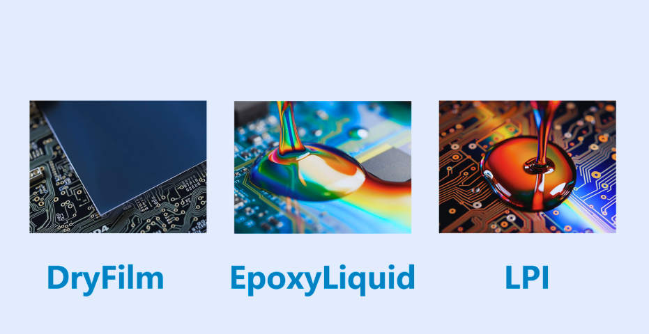
Epoxy Liquid Solder Mask
This is among the most conventional and economically viable solder mask types. Epoxy liquid is applied to the PCB through a screen-printing method and subsequently cured using heat. It is particularly well-suited for less complex designs, offering adequate protection at a lower cost. However, it may not deliver the precise definition required for high-density or fine-pitch component layouts due to potential inconsistencies in thickness and resolution.
Liquid Photoimageable Solder Mask (LPI)
Liquid Photoimageable (LPI) solder mask represents a more advanced solution and is extensively utilized in contemporary PCB manufacturing. Applied as a uniform liquid coating across the entire board, it is then selectively exposed to UV light through a photomask to define the specific areas that are intended to remain masked. The unexposed regions are subsequently washed away, leaving behind precise openings for soldering. LPI offers superior accuracy, making it an ideal choice for intricate designs with tight tolerances, such as those featuring surface-mount components. It also boasts greater durability compared to epoxy liquid masks.
Dry Film Photoimageable Solder Mask
Dry film solder mask is supplied as a solid sheet, which is then laminated onto the PCB surface under controlled heat and pressure. Similar to LPI, it is processed using UV light and a photomask to create precise openings. This type is often preferred for high-resolution applications due to its consistent thickness and excellent adhesion properties. However, its application can be more costly and complex compared to liquid alternatives.
Top and Bottom Side Masks
It is important to note that solder masks are typically applied to both the top and bottom surfaces of a PCB. Each side may have distinct requirements based on the specific components mounted and the overall board layout. In some designs, different mask types or even colors may be employed on each side for functional or aesthetic considerations. The selection of the most suitable solder mask type hinges on factors such as budgetary constraints, the complexity of your PCB design, and the capabilities of your chosen manufacturing partner. For most entry-level designers, LPI is generally a reliable choice due to its balanced combination of precision and cost-effectiveness.
Exploring Popular Solder Mask Colors and Their Practical Uses
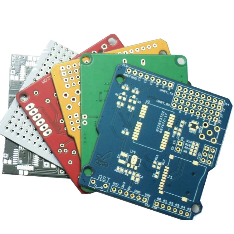
When envisioning a PCB, the iconic green board usually comes to mind. While green remains the traditional and most ubiquitous solder mask color, it is by no means the sole option. Solder mask colors can vary significantly, each serving distinct practical and aesthetic purposes. Let's delve into the most common choices and the rationale behind their application.
Green Solder Mask: The Industry Standard
Green has been the conventional solder mask color for many decades. Its widespread use is primarily attributed to its excellent contrast with white silkscreen labels, which significantly enhances the readability of text and component identifiers. Green also facilitates visual inspections, as subtle defects like scratches or misalignments are easily discernible against its backdrop. Furthermore, it is often the most economical option due to its extensive use and broad compatibility with established manufacturing processes.
Red Solder Mask: A Bold Aesthetic Choice
Red solder masks are frequently selected for their striking visual appeal, imparting a distinctive and vibrant look to the PCB. They are a popular choice in consumer electronics or prototype designs where visual aesthetics are a key consideration. However, red can somewhat impede the detection of defects compared to green, and silkscreen text may not offer optimal contrast unless paired with yellow or another light color.
Blue Solder Mask: A Visually Distinctive Option
Blue solder masks offer another visually appealing alternative, often utilized in branded products or designs aiming for a unique aesthetic. Similar to red, blue may slightly reduce visibility during detailed inspections but can be effectively combined with white or yellow silkscreen for improved legibility.
Black Solder Mask: Specialized for Low Reflection
Black solder masks are less common but find specific applications in areas such as LED displays or optical devices, primarily because they effectively minimize light reflection. A consideration with black is its tendency to absorb more heat, which could potentially impact performance in high-temperature operating environments. Additionally, visual inspections can be more challenging unless bright silkscreen colors are employed for contrast.
White Solder Mask: Optimized for Light Reflection
White solder masks are rare but prove valuable in specific applications, particularly in LED lighting, where they are used to maximize light reflection for enhanced efficiency. A drawback is their tendency to show dirt or defects more prominently, making them less ideal for all projects.
Yellow and Other Custom Colors: For Unique Requirements
Yellow and other less common colors are occasionally utilized for highly specialized or custom design projects. These colors often entail a higher PCB cost and may not integrate as seamlessly with standard manufacturing processes, thus typically being reserved for specific branding objectives or unique functional requirements. While the choice of solder mask color might seem like a minor detail, it can profoundly influence both the functional performance and the visual presentation of your PCB. For novices, adhering to green is generally the safest and most pragmatic option, unless a project dictates specific requirements.
The Fabrication and Application Process of Solder Masks
Understanding how solder masks are manufactured and applied offers valuable insights into the broader PCB production process. While the precise methodology varies depending on the type of solder mask, the general sequence of steps remains broadly similar. Here’s a simplified overview of how solder masks are created and integrated onto a PCB.
Step-by-Step Application Process
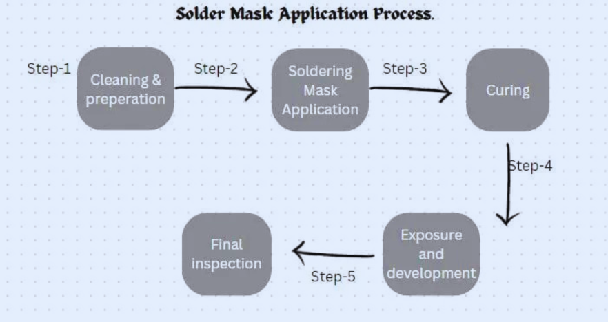
1. PCB Surface Preparation: Prior to solder mask application, the PCB surface must be meticulously cleaned to be entirely free of contaminants. Any presence of dust, oils, or residues on the copper traces can severely impede the proper adhesion of the mask. The board undergoes rigorous cleaning, often involving chemical solutions or abrasive techniques, to ensure an impeccably smooth and clean surface.
2. Solder Mask Material Application: The application method is dictated by the specific solder mask type:
a. Epoxy Liquid: Applied via a screen-printing technique, where the liquid mask is pushed through a fine mesh screen onto the PCB, selectively covering the target areas. This is a relatively simple and cost-effective method but offers less precision.
b. Liquid Photoimageable (LPI): The liquid is either sprayed or rolled uniformly onto the entire PCB surface, creating a thin, even layer. This technique provides superior control over both thickness and coverage.
c. Dry Film: A solid sheet of solder mask material is precisely laminated onto the PCB using controlled heat and pressure. This ensures highly uniform thickness but necessitates more specialized equipment.
3. Pattern Definition (for Photoimageable Masks): For LPI and dry film masks, the subsequent crucial step involves defining which areas of the mask will remain and which will be removed to expose copper for soldering. A photomask—a film imprinted with the desired pattern—is accurately positioned over the board, and the assembly is then exposed to UV light. The UV light causes the solder mask in the exposed areas to harden, while the unexposed regions remain soft and are subsequently removed using a developer solution. This precise photolithographic process creates accurate openings for pads and vias.
4. Solder Mask Curing: Once the mask is applied and patterned, it undergoes a curing process to harden and form a permanent bond with the PCB. This is typically achieved through heat (thermal curing) or additional UV exposure, depending on the specific material's requirements. Curing ensures the mask's resilience to the high temperatures of the soldering process and its durability against environmental stresses.
5. Inspection and Quality Assurance: Following the curing stage, the PCB undergoes a thorough inspection to verify the correct application of the solder mask. Manufacturers scrutinize for potential issues such as incomplete coverage, misalignment, or defects within the openings. Advanced techniques, including Automated Optical Inspection (AOI), are frequently employed to validate quality, particularly in high-volume production environments.
The entire process is meticulously controlled to conform to stringent industry standards, thereby ensuring that the solder mask reliably performs its protective and insulating functions. For beginners, it's beneficial to understand that this crucial step is managed by the PCB manufacturer; however, providing accurate design files with clearly defined solder mask layers is essential to prevent any manufacturing errors.
Key Recommendations for Beginners Working with Solder Masks
If you are new to PCB design, here are some practical tips to keep in mind concerning solder masks.
Essential Design and Communication Advice
● Integrate Solder Mask Layers in Design Files: When submitting your PCB design for manufacturing, ensure that your Gerber files explicitly include clearly defined solder mask layers. This provides the manufacturer with precise instructions on where to apply the mask and where to create openings for soldering.
● Account for Solder Mask Clearance: Design with sufficient clearance around pads—typically 0.1 mm or more, depending on the manufacturer’s capabilities—to prevent overlap or misalignment issues during the mask application process.
● Prioritize Standard Colors for Cost-Efficiency: Unless your project specifically mandates a custom color for branding or unique functional requirements, opting for green will generally help keep costs down and ensure broader compatibility with standard manufacturing procedures.
● Thorough Design Rule Checks (DRC): Utilize your design software’s Design Rule Check (DRC) feature to confirm that your solder mask layers align accurately with the copper layers and adhere to specified manufacturing tolerances. Errors at this stage can lead to critical issues such as exposed traces or pads being inadvertently covered.
● Maintain Open Communication with Your Manufacturer: If you have any uncertainties regarding solder mask options or specific requirements, proactively reach out to your manufacturing partner for expert guidance. They can provide valuable advice on the most suitable type and color for your particular project.
Common Solder Mask Issues and Strategies for Prevention
Even with meticulous planning, solder mask-related issues can arise during manufacturing. Awareness of these potential problems can significantly contribute to designing more robust PCBs. Here are some frequent issues and effective preventative measures.
Troubleshooting and Prevention Strategies
● Solder Mask Misalignment: This occurs when the mask is not accurately aligned with the copper pads, potentially covering areas intended for soldering or leaving traces exposed. To prevent this, ensure your design files are highly accurate and strictly adhere to the manufacturer’s minimum clearance and tolerance specifications.
● Incomplete Coverage: Occasionally, the solder mask may not fully cover its intended areas due to application errors or surface contamination. Partnering with a reliable manufacturer who implements stringent quality control processes is crucial to minimize this risk.
● Peeling or Delamination: Poor adhesion can lead to the solder mask peeling off over time, particularly under harsh operating conditions. This issue can be mitigated by ensuring proper surface preparation and thorough curing during the manufacturing process.
● Color Inconsistencies: If aesthetic consistency is paramount, be aware that custom colors might exhibit slight variations between different manufacturing batches. For critical applications where color uniformity is essential, stick to standard colors or establish clear expectations with your manufacturer.
Conclusion: Mastering the Fundamentals of Solder Masks for Reliable PCBs
A solder mask, though seemingly a minor detail, is an absolutely vital component of any PCB, delivering essential protection, insulation, and precision during the soldering process. For beginners in PCB design, grasping the fundamental aspects of what a solder mask is, its functional importance, the array of available types, popular color choices, and its manufacturing process can profoundly influence the creation of reliable and professional-grade circuit boards. Whether you are developing a simple prototype or preparing for large-scale mass production, meticulous attention to solder mask details is key to ensuring your PCB performs as intended and exhibits enhanced longevity.


