Introduction
Electronics manufacturing faces relentless demands for faster turnaround times, greater customization, and lower costs in an industry driven by rapid innovation cycles. Traditional batch production often leads to excess inventory, prolonged lead times, and increased operational waste, straining resources across the supply chain. Just-in-Time (JIT) PCB production emerges as a transformative approach, drawing from lean manufacturing principles to align fabrication directly with customer demand. This method minimizes stockpiles while maintaining high quality, offering substantial JIT PCB benefits for electric engineers optimizing designs for production. By streamlining processes from panelization to final inspection, JIT enables efficient PCB production that adapts to volatile market needs. Factory-driven implementation of JIT not only enhances responsiveness but also sets new benchmarks for sustainability and precision in PCB manufacturing.

What Is Just-in-Time PCB Production and Why It Matters
Just-in-Time PCB production involves fabricating printed circuit boards precisely when orders are confirmed, eliminating the need for large pre-produced inventories. Rooted in lean manufacturing PCB strategies, JIT pulls materials and processes through the production line based on real-time demand signals rather than push-based forecasting. This shift reduces holding costs associated with raw materials like copper-clad laminates and substrates, which can tie up capital in warehouses. For electric engineers, understanding JIT matters because it directly impacts design-for-manufacturability decisions, such as layer stackups and trace routing optimized for shorter cycles. In high-mix, low-volume scenarios common in prototyping and custom electronics, JIT prevents obsolescence of components and boards due to design revisions. Ultimately, JIT PCB production revolutionizes workflows by fostering a culture of continuous improvement, aligning factory output with end-user requirements.
The relevance of JIT intensifies amid global supply chain disruptions, where traditional methods amplify risks from material shortages. Electric engineers benefit from JIT's emphasis on quality at every stage, ensuring boards meet stringent performance criteria without rework delays. Waste reduction PCB becomes a core outcome, as overproduction and excess motion in material handling are systematically eliminated. This approach supports scalable production for applications ranging from consumer devices to industrial controls, making it indispensable for competitive electronics manufacturing.
Core Principles of JIT in PCB Manufacturing
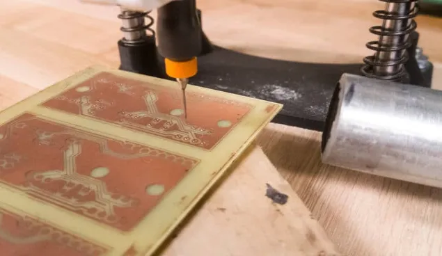
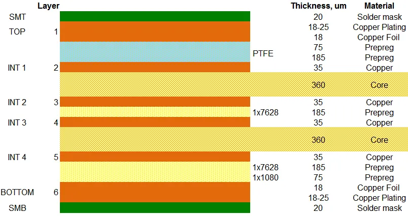
JIT PCB production relies on pull systems, where downstream processes signal upstream activities to initiate work, preventing bottlenecks in etching, drilling, or plating lines. Kanban cards or digital equivalents track work-in-progress (WIP), limiting batches to what the next station can immediately process, thus maintaining flow. Factory floors adopt single-minute exchange of dies (SMED) techniques to reduce setup times between panel runs, enabling rapid switches between multilayer rigid boards and flex circuits. Standardization of processes, guided by adherence to IPC-6012E for qualification and performance of rigid printed boards, ensures consistency despite smaller lot sizes. Electric engineers appreciate how these principles preserve signal integrity and thermal management, as fresh boards avoid storage-induced warpage or delamination.
Lean manufacturing PCB integrates value stream mapping to identify and eliminate non-value-adding steps, such as unnecessary inspections or transport between cleanrooms. Root cause analysis tools like 5-Why help sustain gains by addressing variances in solder mask application or via filling. Supplier synchronization is critical, with vendors delivering pre-cut cores or drilled panels on-demand to feed the line seamlessly. This factory-driven orchestration minimizes defects propagating through lamination or routing, upholding IPC-A-600K acceptability criteria for printed boards. Overall, these mechanisms deliver efficient PCB production by balancing takt time, the rate of customer demand, with actual cycle times.
Implementing JIT PCB Production: Best Practices
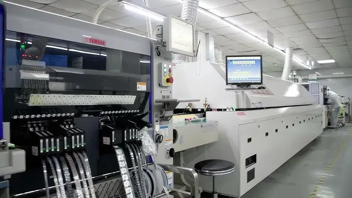
Successful JIT rollout begins with process auditing to baseline current lead times from Gerber file receipt to shipping, targeting reductions through cellular manufacturing layouts. Grouping related operations, like imaging and developing, into U-shaped cells cuts intra-factory travel and enables one-piece flow for high-density interconnect (HDI) boards. Electric engineers should collaborate early, providing design files with embedded manufacturing rules to avoid iterations that disrupt pull signals. Training operators on quick-change tooling for exposure units and developers ensures minimal downtime, while automated optical inspection (AOI) verifies features inline without halting production.
Supplier integration forms the backbone, requiring just-in-time deliveries of base materials certified to JEDEC standards for moisture sensitivity, preventing baking delays. Factories implement daily production meetings to adjust schedules based on order pipelines, incorporating buffer stocks only for long-lead laminates. Waste reduction PCB practices include recycling etchants and optimizing panel utilization to exceed 90% yield through nested routing algorithms. For cost savings PCB manufacturing, track key performance indicators (KPIs) like on-time delivery and first-pass yield, refining setups iteratively. Electric engineers gain from this by receiving prototypes in days, accelerating validation of power distribution networks or impedance-controlled traces.
Challenges such as component variability demand robust quality gates, aligned with ISO 9001:2015 quality management systems to standardize incoming inspections. Addressing these through poka-yoke error-proofing, like fixture-guided drilling, sustains JIT momentum. Factories transitioning to JIT often phase in pilot lines for specific product families, scaling insights across operations.
Key JIT PCB Benefits in Practice
Among the standout JIT PCB benefits is dramatic waste reduction PCB, targeting the seven lean wastes: overproduction, waiting, transport, overprocessing, inventory, motion, and defects. By producing to order, factories avoid scrapped panels from forecast errors, conserving resources like gold plating for edge connectors. Efficient PCB production emerges as lines achieve higher throughput with less floor space, freeing capacity for emerging technologies like embedded components. Cost savings PCB manufacturing accrue from lower capital locked in inventory, reduced energy for climate-controlled storage, and minimized obsolescence in fast-evolving designs.
Quality improvements stem from shorter production windows, where defects are detected and corrected faster via immediate feedback loops. Electric engineers note enhanced reliability, as boards ship fresher, reducing field failures from handling or environmental exposure. Flexibility shines in handling design changes mid-run, supporting agile development for RF modules or sensor interfaces. Lean manufacturing PCB fosters a proactive workforce, empowered to suggest kaizen events that trim plating cycle times or enhance legend printing precision.
Sustainability gains include lower material usage and emissions from optimized transport, aligning with industry pushes for greener electronics. These benefits compound, positioning JIT adopters to meet tight deadlines without compromising on via reliability or solder joint integrity.
Overcoming Challenges in JIT PCB Production
Supply chain volatility poses hurdles, as delays in drill bits or photoresists can starve the line, necessitating diversified sourcing and safety stock calculations based on historical lead times. Factories counter this with vendor scorecards and collaborative forecasting, ensuring alignment without reverting to batching. Workforce adaptability requires cross-training to handle multiple processes, mitigating absenteeism impacts in plating or test areas.
Quality consistency demands rigorous adherence to standards, preventing excursions in copper thickness uniformity. Electric engineers mitigate risks by simulating JIT flows in design software, verifying panel yields pre-production. Digital twins of fab lines predict bottlenecks, enabling proactive adjustments. Through disciplined execution, these solutions unlock full JIT potential.
Conclusion
Just-in-Time PCB production redefines electronics manufacturing by embedding lean principles into every facet, from material intake to final bare board testing. Electric engineers leverage JIT PCB benefits like waste reduction PCB and cost savings PCB manufacturing to iterate designs rapidly and reliably. Efficient PCB production through pull systems and standardized processes ensures high yields and adaptability. Factory-driven insights underscore the need for cultural commitment and supplier partnerships to sustain gains. As demands for compact, high-performance boards grow, JIT positions manufacturers at the forefront of innovation.
FAQs
Q1: What are the primary JIT PCB benefits for electric engineers?
A1: JIT PCB benefits include reduced lead times for prototypes, enabling faster design validation and revisions. Waste reduction PCB minimizes excess materials, lowering costs and environmental impact. Efficient PCB production maintains quality per IPC standards, with fresher boards exhibiting better flatness and reliability. Overall, it supports agile workflows in high-mix environments, aligning fabrication with engineering timelines.
Q2: How does lean manufacturing PCB integrate with JIT production?
A2: Lean manufacturing PCB complements JIT by eliminating non-value steps like unnecessary storage or transport in the fab line. Pull systems synchronize etching, lamination, and routing to demand, cutting inventory costs. Factories achieve cost savings PCB manufacturing through continuous kaizen, optimizing panel nesting and process yields. This integration ensures consistent output for complex multilayer boards.
Q3: What role does efficient PCB production play in waste reduction PCB?
A3: Efficient PCB production under JIT targets overproduction and defects by producing exact quantities, recycling process chemicals where possible. Inline AOI and automated handling reduce motion waste, preserving trace integrity. Adherence to standards like ISO 9001 supports precise process control, minimizing rework. Engineers benefit from streamlined flows that enhance sustainability without sacrificing performance.
Q4: Can JIT address cost savings PCB manufacturing in high-volume runs?
A4: Yes, JIT delivers cost savings PCB manufacturing by slashing inventory holding and obsolescence risks, even in higher volumes via modular lines. Supplier JIT deliveries cut procurement premiums, while SMED shortens setups between runs. Quality focus per J-STD reduces escapes, lowering warranty costs. Electric engineers see value in scalable, responsive production matching demand fluctuations.
References
IPC-6012E — Qualification and Performance Specification for Rigid Printed Boards. IPC, 2017
IPC-A-600K — Acceptability of Printed Boards. IPC, 2020
ISO 9001:2015 — Quality Management Systems. ISO, 2015