Introduction
In the realm of high-speed PCB design, PCB signal integrity stands as a cornerstone for reliable performance. As data rates climb into the gigahertz range, even minor discrepancies in signal paths can lead to failures. Impedance control emerges as a critical strategy to preserve signal quality from source to destination. This article delves into the principles of transmission line impedance, exploring how precise impedance matching mitigates issues like signal reflection. Engineers tackling high-speed interfaces, such as those in telecommunications or computing, rely on these techniques to ensure clean signal propagation. Understanding these fundamentals empowers designers to build robust boards that meet stringent performance demands.
What Is Transmission Line Impedance in PCBs?
Transmission line impedance refers to the characteristic impedance of conductive traces on a PCB, determined by their geometry and the surrounding dielectric materials. In high-speed PCB design, traces behave as transmission lines where signals propagate as electromagnetic waves. The impedance, typically 50 ohms for single-ended lines or 100 ohms for differential pairs, must remain consistent along the entire path. Factors like trace width, thickness, dielectric height, and material properties directly influence this value. When controlled properly, it enables efficient power transfer without distortion. Deviations lead to mismatches, compromising PCB signal integrity.
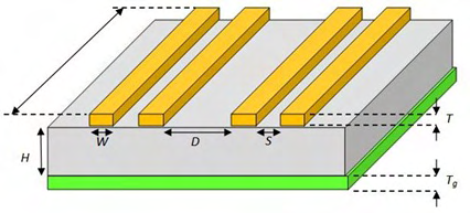
Microstrip and stripline configurations represent common transmission line types in PCBs. Microstrips sit on the outer layers with air and dielectric above and below, while striplines are embedded between ground planes. Each setup requires tailored design parameters to achieve target impedance. Engineers calculate these using established equations that account for effective dielectric constants. Consistent impedance ensures that signals maintain their shape, avoiding attenuation or ringing. This control forms the basis for reliable high-speed signaling.
Why Impedance Control Matters for High-Speed PCB Design
High-speed PCB design demands impedance control to prevent signal reflection, which occurs when impedance mismatches cause portions of the signal to bounce back toward the source. Reflections distort waveforms, leading to overshoot, undershoot, and timing errors that degrade eye diagrams. In applications like DDR memory or PCIe interfaces, these effects can cause bit errors or system instability. Impedance matching aligns the source, trace, and load impedances, maximizing power transfer as per transmission line theory. Without it, signals lose fidelity over distance, especially beyond rise time limits. Thus, impedance control directly safeguards PCB signal integrity in modern electronics.
As frequencies increase, the electrical length of traces approaches wavelengths, amplifying mismatch effects. Short traces may tolerate variations, but high-speed designs exceed critical lengths where full-wave behavior dominates. Standards like IPC-2221 provide guidelines for trace dimensions to support impedance control. Engineers must consider not just nominal values but also tolerances during fabrication. Poor control escalates electromagnetic interference and crosstalk between adjacent lines. Prioritizing impedance from the layout stage yields boards that perform predictably in real-world conditions.
Fundamental Principles of Transmission Line Impedance
The characteristic impedance Z0 of a transmission line derives from its inductance L and capacitance C per unit length, given by Z0 = sqrt(L/C). For microstrips, IPC-2141 outlines equations incorporating trace width W, dielectric thickness H, and relative permittivity Er. These formulas enable predictive modeling before fabrication. Variations in Er due to material inconsistencies alter Z0, underscoring the need for stable dielectrics. Engineers simulate stackups to balance these parameters for target impedances. This principled approach underpins effective impedance matching.
Dielectric materials contribute significantly to transmission line impedance through their Er values, typically 3.5 to 4.5 for common FR-4 laminates. Higher Er lowers impedance for fixed geometries, while thinner dielectrics increase it. Copper roughness and plating thickness introduce minor perturbations at high frequencies. Ground plane proximity affects field distribution, making symmetric stackups preferable for striplines. Understanding these interactions allows precise design adjustments. Ultimately, these principles guide high-speed PCB design toward optimal signal integrity.
Achieving Impedance Matching in PCB Design
Impedance matching begins with stackup planning, where layer thicknesses and materials are selected to support target Z0 values. Designers widen traces or adjust spacing for differential pairs to hit 100 ohms differential impedance. Reference planes provide return paths, minimizing loop inductance. Vias introduce discontinuities, so back-drilling or stub management mitigates stubs. Simulations validate designs against fabrication tolerances, typically ±10% for impedance. This systematic process ensures transmission line impedance consistency across the board.
Routing strategies further enhance matching by avoiding sharp bends that alter effective width. Length matching for differential pairs preserves phase alignment, crucial for common-mode rejection. Termination resistors at ends absorb reflections in source-terminated schemes. Engineers employ field solvers for accuracy beyond analytical models. Fabricators confirm via test coupons on panels. These combined efforts deliver PCBs ready for high-speed operation.
Common Causes of Signal Reflection and Mitigation
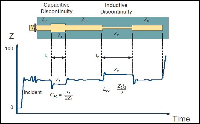
Signal reflection arises primarily from abrupt impedance changes, such as at vias, connectors, or plane splits. When Z0 shifts, the reflection coefficient Γ = (Z2 - Z1)/(Z2 + Z1) quantifies the bounced voltage fraction. For a 50-ohm line meeting a 75-ohm section, Γ = 0.2, causing 20% reflection. High-speed edges exacerbate this via fast rise times. Identifying hotspots through time-domain reflectometry (TDR) pinpoints issues. Proactive design minimizes these risks.
Other contributors include etch variations and solder mask effects, which slightly raise effective Er. Plane voids force signals to detour, increasing inductance. Crosstalk from unshielded neighbors couples noise, mimicking reflections. IPC-6012 specifies performance criteria, including impedance tolerances for qualified boards. Mitigation involves dense stitching vias around transitions and continuous reference planes. Regular verification maintains PCB signal integrity.
Best Practices for Impedance Control in Manufacturing
Specify impedance tolerances in fabrication notes, aiming for ±10% or tighter for critical nets. Test coupons with microstrip and stripline samples validate process capability. TDR or vector network analyzers measure Z0 post-etch. Adjust etch factors to compensate for under-etching that widens traces. Material preconditioning stabilizes Er against humidity. These practices align production with design intent.
Multilayer stackups demand tight control of prepreg and core thicknesses. Symmetric builds prevent warpage that stresses traces. Fabricators use flying probe testers for inline checks. Documentation traces lots for traceability. Adhering to these elevates high-speed PCB design reliability.
Troubleshooting Impedance-Related Signal Integrity Issues
When eye diagrams show closure, suspect mismatches first. TDR scans reveal step changes along traces. Simulate with extracted geometries to correlate. Adjust terminations or reroute if feasible. For prototypes, measure S-parameters to quantify reflections. Iterative fixes restore margins.
Fabrication variances often underlie field failures. Review coupons against specs. Material swaps require recalibration. Collaborate with fabricators on process tweaks. This diagnostic mindset resolves most issues efficiently.
Conclusion
Impedance control unlocks PCB signal integrity by ensuring consistent transmission line impedance throughout high-speed designs. From stackup planning to testing, each step counters signal reflection through precise impedance matching. Engineers applying these principles, guided by standards like IPC-2141 and IPC-6012, produce reliable boards. Proactive design and verification minimize risks, enabling robust performance. Mastering these techniques positions teams to meet escalating speed demands effectively.
FAQs
Q1: What is transmission line impedance in the context of PCB signal integrity?
A1: Transmission line impedance is the characteristic impedance of PCB traces, calculated from inductance and capacitance per unit length. It ensures signals propagate without distortion in high-speed PCB design. Consistent values, like 50 ohms single-ended or 100 ohms differential, prevent reflections. Factors such as trace geometry and dielectric properties define it. Proper control maintains waveform integrity across interfaces.
Q2: How does impedance mismatch lead to signal reflection in PCBs?
A2: Impedance mismatch occurs when trace, source, or load Z0 values differ, causing partial signal reflection per the reflection coefficient formula. This distorts waveforms, introducing ringing and jitter that harm PCB signal integrity. In high-speed designs, fast edges amplify effects, closing eye openings. Matching impedances absorbs energy fully at terminations. TDR identifies mismatch locations for correction.
Q3: What are key best practices for impedance matching in high-speed PCB design?
A3: Start with stackup optimization for target Z0, using simulations for microstrip and stripline geometries. Route with length matching for pairs and avoid discontinuities. Specify tolerances and test via coupons. Employ reference planes and stitching vias. Verify with TDR post-fabrication. These ensure transmission line impedance consistency and robust signal integrity.
Q4: How can engineers test and verify PCB impedance control?
A4: Use TDR to measure Z0 along traces, detecting variations from ideal. Network analyzers provide S11 return loss data. Include test coupons on panels for process validation. Compare against design specs, typically ±10%. Pre- and post-laminate checks confirm stability. This verifies impedance matching for high-speed performance.
References
IPC-2141A — Design Guide for High-Speed Controlled Impedance Circuit Boards. IPC, 1996
IPC-2221B — Generic Standard on Printed Board Design. IPC, 2012
IPC-6012E — Qualification and Performance Specification for Rigid Printed Boards. IPC, 2017


